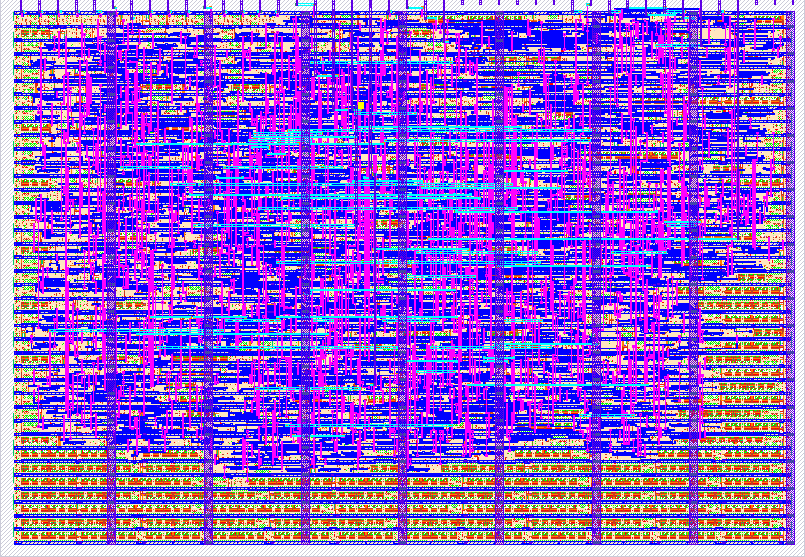
170 Clock Domain Crossing FIFO
170 : Clock Domain Crossing FIFO

- Author: Kenneth Wilke
- Description: This FIFO buffers 4-bits data asynchronously across clock domains
- GitHub repository
- Open in 3D viewer
- Clock: 0 Hz
How it works
This is a FIFO that can pass data asynchronously across clock domains. This was a project I created when I was first learning logic design, and it took me a couple weeks to settle on a design that I felt was clean and reusable.
The FIFO can hold 32 4-bit values, or 16 bytes. So use them wisely and greatly!
The original design can be found at https://github.com/KennethWilke/sv-cdc-fifo
The architecture of this design was influenced by this paper written by Clifford E. Cummings of Sunburst Design but the implementation was fully written by me.
How to test
Hold write_reset and read_reset LOW while running the clock for a bit to reset, then raise to initialize the module.
Writing to the FIFO
Prepare your data on the 4-bit write_data bus, ensure the full state is low and then raise write_increment for 1 cycle of write_clock to write data into the FIFO memory.
Reading from the FIFO
The FIFO will present the current output on the read_data bus. If empty is low, this output should be valid and you can acknowledge receive of this vallue by raising read_increment for 1 cycle of read_clock.
IO
| # | Input | Output | Bidirectional |
|---|---|---|---|
| 0 | write_clock | empty | write_reset |
| 1 | write_increment | full | read_reset |
| 2 | read_clock | ||
| 3 | read_increment | ||
| 4 | write_data0 | read_data0 | |
| 5 | write_data1 | read_data1 | |
| 6 | write_data2 | read_data2 | |
| 7 | write_data3 | read_data3 |