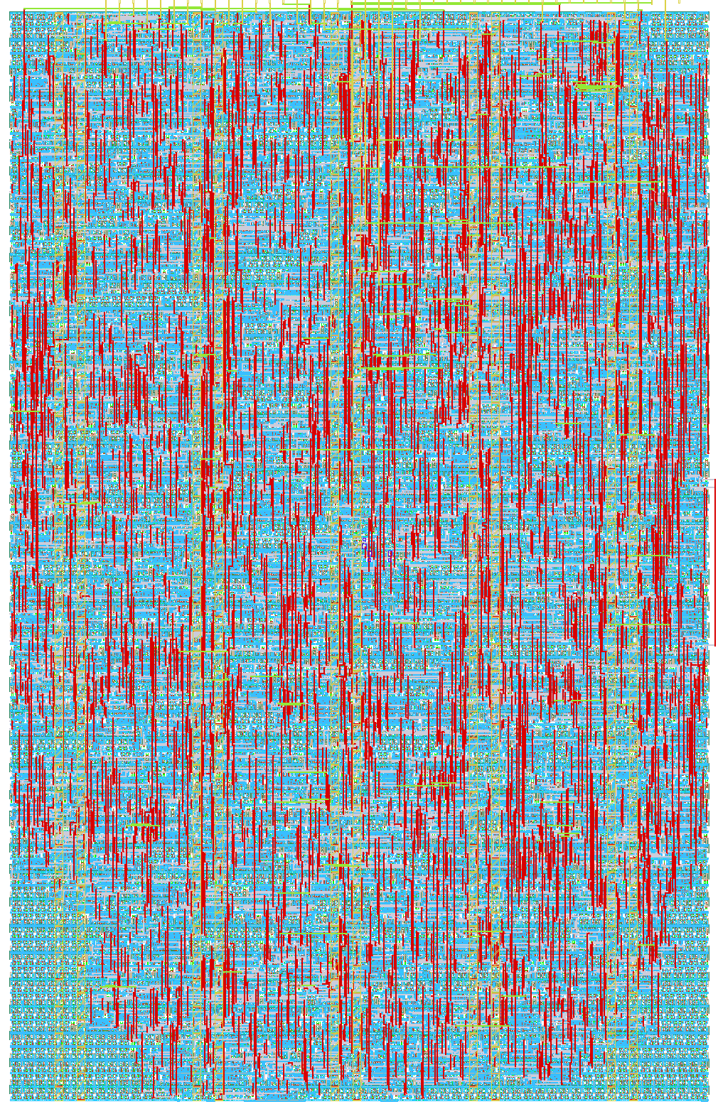
257 Delta Sigma Comparator Based ADC
257 : Delta Sigma Comparator Based ADC

- Author: Pawel Kozlowski
- Description: Evaluating the feasibility of implementing a delta-sigma analog-to-digital conversion using two switched-capacitor lines. One line serves as a reference, while the other is intended for current measurement, such as from a photodiode. The project also explores how process, voltage, and temperature (PVT) variations affect flip-flop behavior, whether these effects can be mitigated through the reference channel, and what additional insights or phenomena may emerge from this investigation.
- GitHub repository
- Open in 3D viewer
- Clock: 10000000 Hz
How it works
This project explores the implementation of a delta-sigma ADC entirely in a digital environment. A flip-flop is used as the quantizer. Due to the strong DVT (device voltage threshold) dependency of flip-flops, a reference line is introduced. Assuming identical behavior across flip-flops, this helps mitigate vDVT variance.
Of course, in practice, flip-flops and capacitors are never perfectly matched. The goal is to evaluate how these mismatches affect ADC linearity, beyond the non-linearity introduced by the RC constant, and to observe the threshold behavior of the flip-flops. This is a quick, exploratory project, so some assumptions may be oversimplified or incorrect. However, in digital simulations, the concept appears to function as intended.
Implementing this on-chip (rather than on an FPGA) offers better control over parasitics at the silicon level, which could improve overall conversion accuracy.
The data output is 13 bits wide, but only 12 bits are effectively used. This is to account for potential overflow, especially in cases where simulation might not catch it. Additionally, since the system operates in bipolar mode, one more bit is reserved to represent the sign. As a result, the effective resolution of the ADC is 11 bits.
How to test
Start by defining the current range to be measured. For example, if the range is 0–100 µA, the baseline of the delta-sigma oscillation should be around 0.6 V (half of a 1.2 V supply). This gives:
R1 = Vc2 / I = 0.6 / (100e-6) = 6000 Ω
The current sink could a reverse-biased photodiode (as shown on the diagram below), but an SMU (source measure unit) can also be used to characterise the system. The circuit is designed to operate in bipolar mode, meaning it can measure both positive and negative currents.
To begin operating the system, first connect the discrete components — resistors, capacitors, and a current source or sink. Once all components are connected, perform a system reset. After resetting, verify that both capacitor lines produce similar values (filtered_a and filtered_b) even without applying an external current source or sink. This confirms the system is functioning correctly. If the outputs are as expected, you can proceed to apply a current with your chosen polarity to begin active operation.
To start data acquisition, send a pulse in the clk clock domain to uio__in[7]. This will trigger the transmission of three filtered data signals in the next clock cycle: filtered_a, filtered_b, and filtered_ab_subtr. For synchronisation, a valid_out signal is sent during the transmission of the first bit of data. This simple approach was chosen to simplify the implementation.
If the internal logic for data transmission fails, components like the CIC filter can be implemented on an FPGA. This can be done by routing the inverter output not only to the capacitor but also to the FPGA. Be mindful of additional parasitics introduced in this setup.
External hardware
- Two identical capacitors: Test values ranging from picofarads to nanofarads. A similar analog-based design supported values from 30 pF (resulting in higher peaks between clock cycles) up to 1300 pF or more.
- Two identical resistors, e.g., 6000 Ω.
- A current source/sink
IO
| # | Input | Output | Bidirectional |
|---|---|---|---|
| 0 | Capacitor a input port | pdm_a - pulse density modulated signal connected to capacitor a | |
| 1 | Capacitor b input port | pdm_b - pulse density modulated signal connected to capacitor a | |
| 2 | filtered_a - 13 bit value of a line after summing (13 to avoid overflow) | ||
| 3 | filtered_b - 13 bit value of b line after summing | ||
| 4 | filtered_ab_subtr represents the difference between the 'a' and 'b' lines after summation (i.e., a - b). The direction of current flow (or polarity), which determines how each capacitor is connected to the respective UI input, must align with this formula to prevent overflow or incorrect charge accumulation. | ||
| 5 | filtered_a valid signal saying that from this bit on the user can expect the integrated value from the first capacitor line | ||
| 6 | filtered_b valid signal saying that from this bit on the user can expect the integrated value from the second capacitor line | ||
| 7 | Data triggger for adc data streaming. Asserting it causes filtered_a, filtered_b and filtered_ab_subtr to be serialised and sent. | filtered_ab_subtr valid signal saying that from this bit on one can expect the difference between the vaules (effectively the ADC code) |