269 Dickson Charge Pump
269 : Dickson Charge Pump
- Author: Uri Shaked
- Description: Pumps the input voltage up to ~3.65V
- GitHub repository
- Open in 3D viewer
- Clock: 2000000 Hz
How it works
A 3-stage dickson charge pump. The output voltage is Vout = 4*(VPWR - Vd) = ~3.6 V where VPWR is the digital input voltage (1.8 V), and Vd is the diode drop (~0.9 V). The output voltage is divided by two and available at the ua[0] pin.
How to test
Apply a clock signal of 2 MHz to the clk input. In TT07, the analog pin voltage is limited to VDDIO/VDDA (usually 3.3 V), so the output voltage will be divided by two. You can measure the divided output voltage at the ua[0] (vout_div) pin.
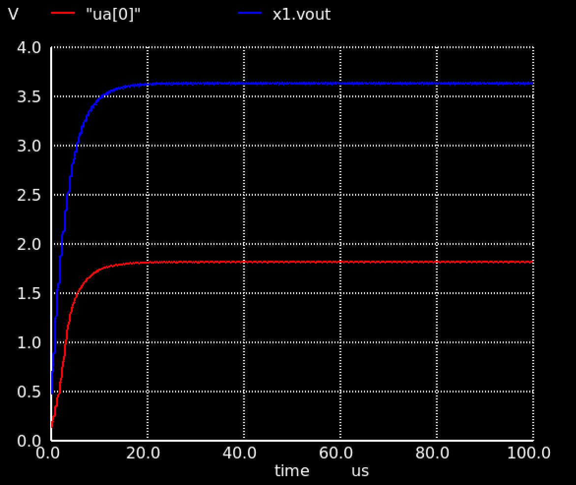
Simulation results
Post layout simulation showing the output voltage x1.vout and the divided output voltage on ta ua[0] pin. The output voltage stabilizes at ~3.65 V, and the divided output voltage at ~1.82 V. The current draw is about 623.5 nA (measured by adding a 1k resistor between ua[0] and VGND in simulation).
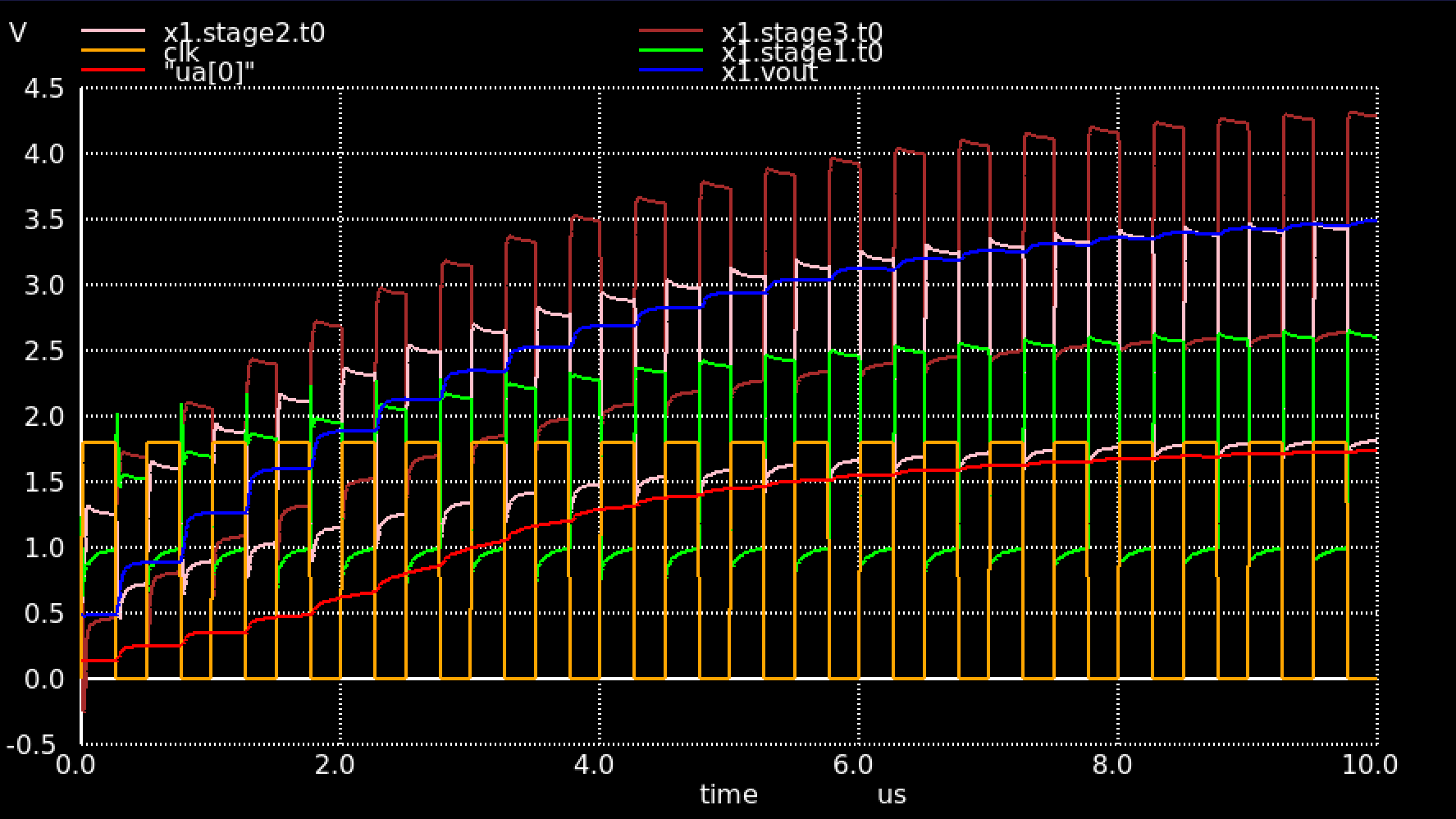
The following graph shows the input clock, the intermediate voltages at the output of each stage, the output voltage, and the divided voltage as they rise during the first 10 us of operation.
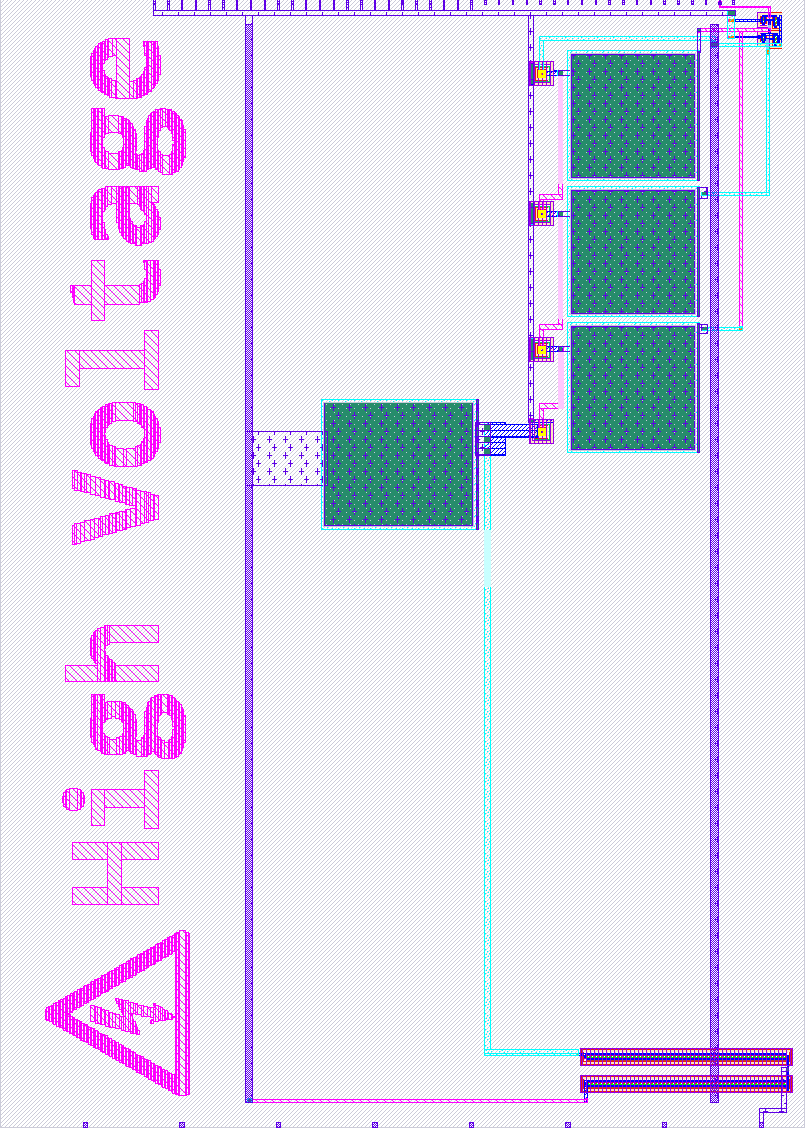
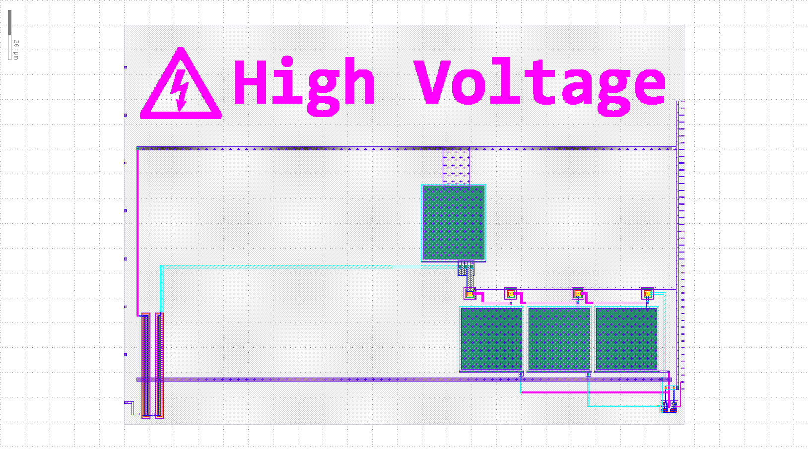
Project layout
IO
| # | Input | Output | Bidirectional |
|---|---|---|---|
| 0 | |||
| 1 | |||
| 2 | |||
| 3 | |||
| 4 | |||
| 5 | |||
| 6 | |||
| 7 |
Analog pins
ua | PCB Pin | Internal index | Description |
|---|---|---|---|
| 0 | B3 | 9 | vout_div |