105 Avalon Semiconductors '5401' 4-bit Microprocessor
105 : Avalon Semiconductors '5401' 4-bit Microprocessor

- Author: Tholin
- Description: 4-bit CPU capable of addressing 4096 bytes program memory and 254 words data memory, with 6 words of on-chip RAM and two general-purpose input ports. Hopefully capable of more complex computation than previous CPU submissions.
- GitHub repository
- Open in 3D viewer
- Clock: 6000 Hz
How it works
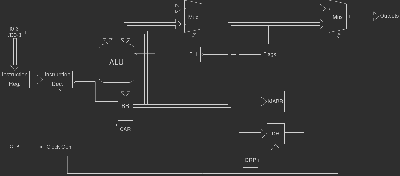
The chip contains a 4-bit ALU, a 4-bit Accumulator, 8-bit Memory Address Register and 12-bit ˝Destination Register˝, which is used to buffer branch target addresses. It also has two general-purpose input ports. The instruction set consists of 16 instructions, containing arihmatic, logical, load/store, branch and conditional branch instruction. See the full documentation for a complete architectural description.
How to test
It is possible to test the CPU using a debounced push button as the clock, and using the DIP switches on the PCB to key in instructions manually. Set the switches to 0100_0000 to assert RST, and pulse the clock a few times. Then, change the switches to 0000_1000 (SEI instruction) and pulse the clock four times. After that, set the switches to all 0s (LD instruction). Pulse the clock once, then change the switches to 0001_0100, and pulse the clock three more times. Lastly, set the switches to 0011_1100 (LMH instruction). If done correctly, after two pulses of the clock, the outputs will read 0101_0000 and two more pulses after that, they will be xxxx_1000 (’x’ means don’t care). This sequence should repeat for as long as you keep pulsing the clock, without changing the inputs.
External hardware
At the very minimum a program memory, and the required glue logic. See ˝Example system diagram˝ in the full documentation.

IO
| # | Input | Output |
|---|---|---|
| 0 | CLK | MAR0 / DR0 / DR8 / RR0 |
| 1 | RST | MAR1 / DR1 / DR9 / RR1 |
| 2 | I0 / D0 | MAR2 / DR2 / DR10 / RR2 |
| 3 | I1 / D1 | MAR3 / DR3 / DR11 / RR3 |
| 4 | I2 / D2 | MAR4 / DR4 / F_MAR |
| 5 | I3 / D3 | MAR5 / DR5 / F_WRITE |
| 6 | EF0 | MAR6 / DR6 / F_JMP |
| 7 | EF1 | MAR7 / DR7 / F_I |