69 S4GA: Super Slow Serial SRAM FPGA
69 : S4GA: Super Slow Serial SRAM FPGA
- Author: Jan Gray(TT02), Marco Merlin (TT03)
- Description: one fracturable 5-LUT that receives FPGA LUT configuration frames, serially evaluates LUT inputs and LUT outputs
- GitHub repository
- Open in 3D viewer
- Clock: 0 Hz
How it works
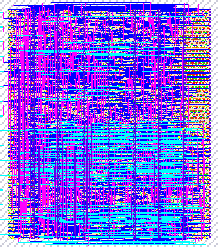
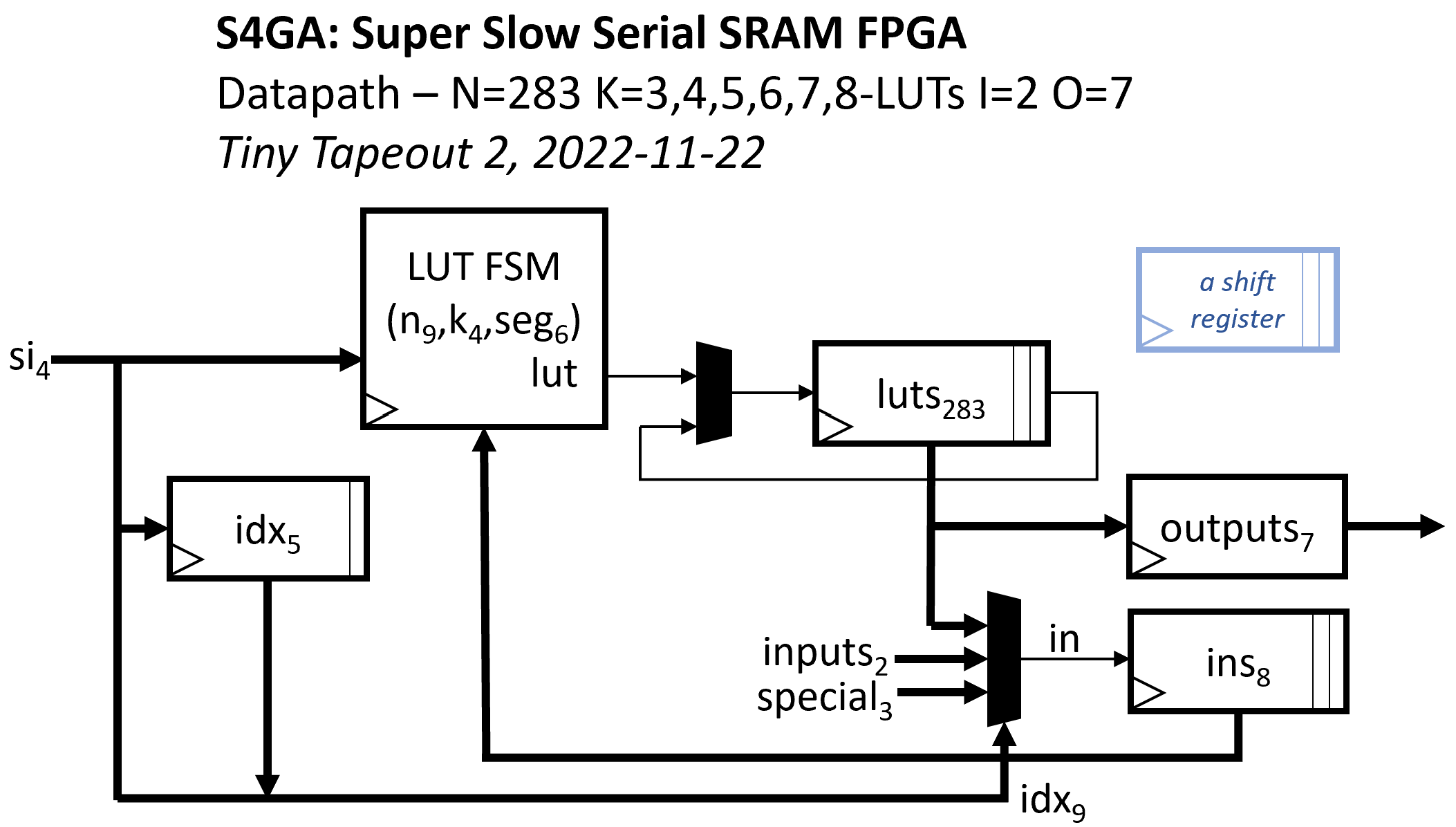
The design is a single physical LUT into which an external agent pours a series of 92b LUT configuration frames, four bits per cycle. Every 23 clock cycles it evaluates a 5-input LUT. The last N=283 LUT output values are kept on die to be used as LUT inputs of subsequent LUTs. The design also has 2 FPGA input pins and 7 FPGA output pins.
How to test
tricky
External hardware
serial SRAM or FLASH
IO
| # | Input | Output |
|---|---|---|
| 0 | clk | out[0] |
| 1 | rst | out[1] |
| 2 | si[0] | out[2] |
| 3 | si[1] | out[3] |
| 4 | si[2] | out[4] |
| 5 | si[3] | out[5] |
| 6 | in[0] | out[6] |
| 7 | in[1] | debug |