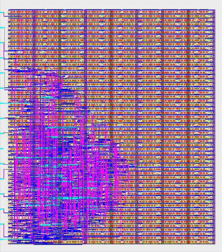
203 FROG 4-Bit CPU
203 : FROG 4-Bit CPU

- Author: ChrisPVille
- Description: The FROG is an extremely minimal load-store 4-bit CPU
- GitHub repository
- Open in 3D viewer
- Clock: 0 Hz
How it works
The CPU addresses external memory on its addr pins and executes/interprets data on the data_in pins
How to test
Set data_in to 0x8 (NOP) and observe the addr bus count upward as the CPU executes Instructions
External hardware
An SRAM/ROM like memory containing instructions should be connected to addr/wcyc/data_in
IO
| # | Input | Output |
|---|---|---|
| 0 | clock | addr[0] |
| 1 | reset_p | addr[1] |
| 2 | data_in[0] | addr[2] |
| 3 | data_in[1] | addr[3] |
| 4 | data_in[2] | addr[4] |
| 5 | data_in[3] | addr[5] |
| 6 | addr[6] | |
| 7 | fast - zero wait state memory mode | write memory cycle |