45 MicroTapeout (of sky130 cells)
45 : MicroTapeout (of sky130 cells)
- Author: htfab
- Description: 395 standard cells with a mux to select between them
- GitHub repository
- Open in 3D viewer
- Clock: 10000 Hz
How it works
Digital chip designs are usually written in a hardware description language like RTL Verilog and then synthesized into a set of mask layers suitable for fabrication. In order to make both synthesis and verification robust for huge designs, a modular approach is used where the functionality of the circuit is decomposed into pre-built blocks called standard cells with well-known and thoroughly tested behaviour and layout.
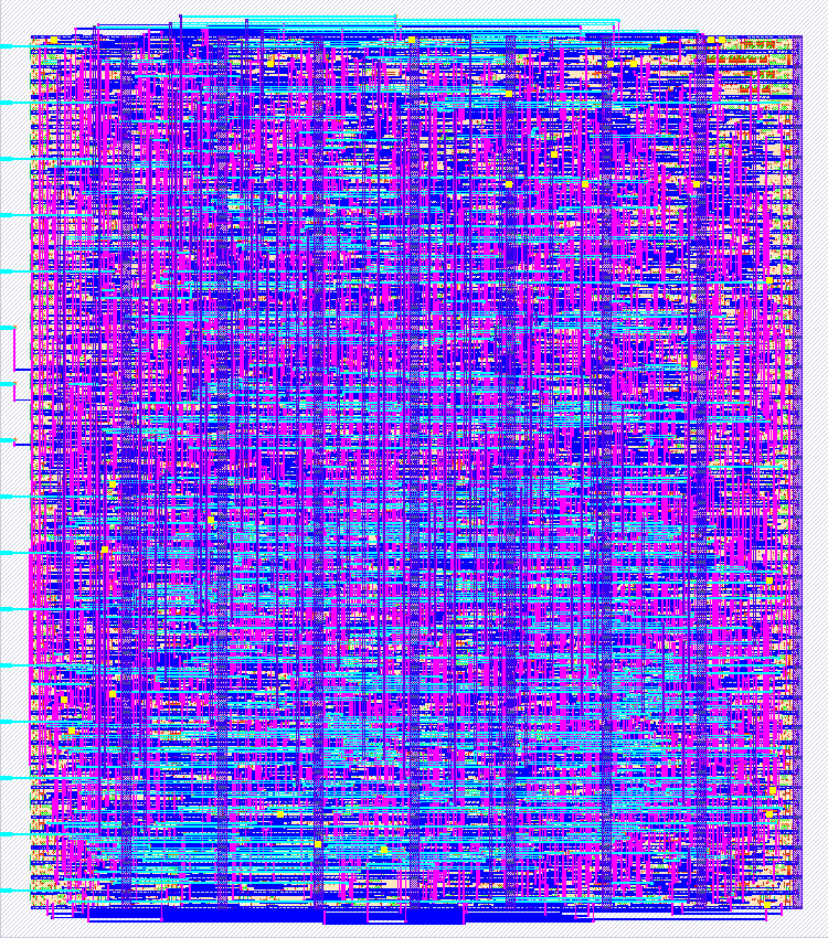
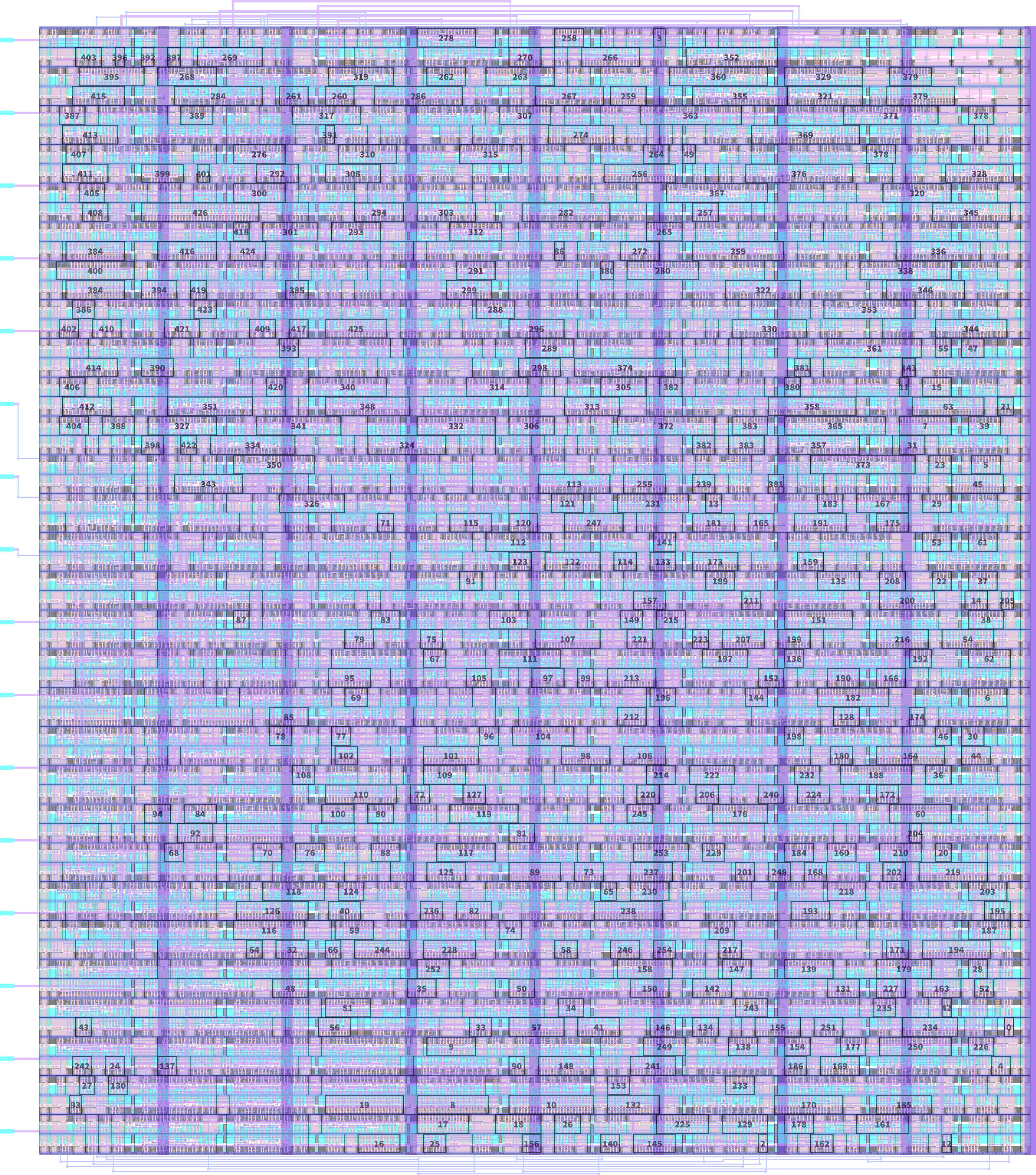
This design contains a copy of most standard cells in the sky130_fd_sc_hd library along with a multiplexing mechanism that allows exposing any of them to the input/output pins.
An MPW shuttle fabricates multiple designs on the same wafer. TinyTapeout merges several projects in a single shuttle submission. MicroTapeout pushes the limit with each block containing just a single cell. Apart from the geek factor the fabricated chip can be used by low-level digital design engineers to better understand the behaviour of the individual standard cells and might even provide some timing insights.
There are 437 standard cells in our library, of which 42 don't produce output or require special power handling. This leaves us with 395 cells. Each cell has up to 6 inputs and up to 2 outputs for a total of 427 outputs. The same 6 inputs are fed into each cell in parallel while the 427 outputs are divided into 54 pages of 8 outputs each with a multiplexer deciding which page is mapped to the output pins.
In order to drive the 6 cell inputs and the 6 bits of input to the mux from a total of 8 input pins we use some registered logic. Input pin 0 is a clock signal while input pin 1 selects page mode. On each rising clock edge we save input pins 2 to 7 into a page register if page mode is on and into an input register if page mode is off. Cell inputs are then supplied from the input register and the mux operates on the page register.
Mapping of outputs to pages:
| page | pin | pin 0/4 | pin 1/5 | pin 2/6 | pin 3/7 |
|---|---|---|---|---|---|
| 000000 | 0-3 | conb_1.h | conb_1.l | buf_1 | buf_2 |
| 4-7 | buf_4 | buf_6 | buf_8 | buf_12 | |
| 000001 | 0-3 | buf_16 | bufbuf_8 | bufbuf_16 | inv_1 |
| 4-7 | inv_2 | inv_4 | inv_6 | inv_8 | |
| 000010 | 0-3 | inv_12 | inv_16 | bufinv_8 | bufinv_16 |
| 4-7 | and2_0 | and2_1 | and2_2 | and2_4 | |
| 000011 | 0-3 | and2b_1 | and2b_2 | and2b_4 | and3_1 |
| 4-7 | and3_2 | and3_4 | and3b_1 | and3b_2 | |
| 000100 | 0-3 | and3b_4 | and4_1 | and4_2 | and4_4 |
| 4-7 | and4b_1 | and4b_2 | and4b_4 | and4bb_1 | |
| 000101 | 0-3 | and4bb_2 | and4bb_4 | nand2_1 | nand2_2 |
| 4-7 | nand2_4 | nand2_8 | nand2b_1 | nand2b_2 | |
| 000110 | 0-3 | nand2b_4 | nand3_1 | nand3_2 | nand3_4 |
| 4-7 | nand3b_1 | nand3b_2 | nand3b_4 | nand4_1 | |
| 000111 | 0-3 | nand4_2 | nand4_4 | nand4b_1 | nand4b_2 |
| 4-7 | nand4b_4 | nand4bb_1 | nand4bb_2 | nand4bb_4 | |
| 001000 | 0-3 | or2_0 | or2_1 | or2_2 | or2_4 |
| 4-7 | or2b_1 | or2b_2 | or2b_4 | or3_1 | |
| 001001 | 0-3 | or3_2 | or3_4 | or3b_1 | or3b_2 |
| 4-7 | or3b_4 | or4_1 | or4_2 | or4_4 | |
| 001010 | 0-3 | or4b_1 | or4b_2 | or4b_4 | or4bb_1 |
| 4-7 | or4bb_2 | or4bb_4 | nor2_1 | nor2_2 | |
| 001011 | 0-3 | nor2_4 | nor2_8 | nor2b_1 | nor2b_2 |
| 4-7 | nor2b_4 | nor3_1 | nor3_2 | nor3_4 | |
| 001100 | 0-3 | nor3b_1 | nor3b_2 | nor3b_4 | nor4_1 |
| 4-7 | nor4_2 | nor4_4 | nor4b_1 | nor4b_2 | |
| 001101 | 0-3 | nor4b_4 | nor4bb_1 | nor4bb_2 | nor4bb_4 |
| 4-7 | xor2_1 | xor2_2 | xor2_4 | xor3_1 | |
| 001110 | 0-3 | xor3_2 | xor3_4 | xnor2_1 | xnor2_2 |
| 4-7 | xnor2_4 | xnor3_1 | xnor3_2 | xnor3_4 | |
| 001111 | 0-3 | a2111o_1 | a2111o_2 | a2111o_4 | a2111oi_0 |
| 4-7 | a2111oi_1 | a2111oi_2 | a2111oi_4 | a211o_1 | |
| 010000 | 0-3 | a211o_2 | a211o_4 | a211oi_1 | a211oi_2 |
| 4-7 | a211oi_4 | a21bo_1 | a21bo_2 | a21bo_4 | |
| 010001 | 0-3 | a21boi_0 | a21boi_1 | a21boi_2 | a21boi_4 |
| 4-7 | a21o_1 | a21o_2 | a21o_4 | a21oi_1 | |
| 010010 | 0-3 | a21oi_2 | a21oi_4 | a221o_1 | a221o_2 |
| 4-7 | a221o_4 | a221oi_1 | a221oi_2 | a221oi_4 | |
| 010011 | 0-3 | a222oi_1 | a22o_1 | a22o_2 | a22o_4 |
| 4-7 | a22oi_1 | a22oi_2 | a22oi_4 | a2bb2o_1 | |
| 010100 | 0-3 | a2bb2o_2 | a2bb2o_4 | a2bb2oi_1 | a2bb2oi_2 |
| 4-7 | a2bb2oi_4 | a311o_1 | a311o_2 | a311o_4 | |
| 010101 | 0-3 | a311oi_1 | a311oi_2 | a311oi_4 | a31o_1 |
| 4-7 | a31o_2 | a31o_4 | a31oi_1 | a31oi_2 | |
| 010110 | 0-3 | a31oi_4 | a32o_1 | a32o_2 | a32o_4 |
| 4-7 | a32oi_1 | a32oi_2 | a32oi_4 | a41o_1 | |
| 010111 | 0-3 | a41o_2 | a41o_4 | a41oi_1 | a41oi_2 |
| 4-7 | a41oi_4 | o2111a_1 | o2111a_2 | o2111a_4 | |
| 011000 | 0-3 | o2111ai_1 | o2111ai_2 | o2111ai_4 | o211a_1 |
| 4-7 | o211a_2 | o211a_4 | o211ai_1 | o211ai_2 | |
| 011001 | 0-3 | o211ai_4 | o21a_1 | o21a_2 | o21a_4 |
| 4-7 | o21ai_0 | o21ai_1 | o21ai_2 | o21ai_4 | |
| 011010 | 0-3 | o21ba_1 | o21ba_2 | o21ba_4 | o21bai_1 |
| 4-7 | o21bai_2 | o21bai_4 | o221a_1 | o221a_2 | |
| 011011 | 0-3 | o221a_4 | o221ai_1 | o221ai_2 | o221ai_4 |
| 4-7 | o22a_1 | o22a_2 | o22a_4 | o22ai_1 | |
| 011100 | 0-3 | o22ai_2 | o22ai_4 | o2bb2a_1 | o2bb2a_2 |
| 4-7 | o2bb2a_4 | o2bb2ai_1 | o2bb2ai_2 | o2bb2ai_4 | |
| 011101 | 0-3 | o311a_1 | o311a_2 | o311a_4 | o311ai_0 |
| 4-7 | o311ai_1 | o311ai_2 | o311ai_4 | o31a_1 | |
| 011110 | 0-3 | o31a_2 | o31a_4 | o31ai_1 | o31ai_2 |
| 4-7 | o31ai_4 | o32a_1 | o32a_2 | o32a_4 | |
| 011111 | 0-3 | o32ai_1 | o32ai_2 | o32ai_4 | o41a_1 |
| 4-7 | o41a_2 | o41a_4 | o41ai_1 | o41ai_2 | |
| 100000 | 0-3 | o41ai_4 | maj3_1 | maj3_2 | maj3_4 |
| 4-7 | mux2_1 | mux2_2 | mux2_4 | mux2_8 | |
| 100001 | 0-3 | mux2i_1 | mux2i_2 | mux2i_4 | mux4_1 |
| 4-7 | mux4_2 | mux4_4 | ha_1.c | ha_1.s | |
| 100010 | 0-3 | ha_2.c | ha_2.s | ha_4.c | ha_4.s |
| 4-7 | fa_1.c | fa_1.s | fa_2.c | fa_2.s | |
| 100011 | 0-3 | fa_4.c | fa_4.s | fah_1.c | fah_1.s |
| 4-7 | fahcin_1.c | fahcin_1.s | fahcon_1.c | fahcon_1.s | |
| 100100 | 0-3 | dlxtp_1 | dlxbp_1.q | dlxbp_1.n | dlxtn_1 |
| 4-7 | dlxtn_2 | dlxtn_4 | dlxbn_1.q | dlxbn_1.n | |
| 100101 | 0-3 | dlxbn_2.q | dlxbn_2.n | dlrtp_1 | dlrtp_2 |
| 4-7 | dlrtp_4 | dlrbp_1.q | dlrbp_1.n | dlrbp_2.q | |
| 100110 | 0-3 | dlrbp_2.n | dlrtn_1 | dlrtn_2 | dlrtn_4 |
| 4-7 | dlrbn_1.q | dlrbn_1.n | dlrbn_2.q | dlrbn_2.n | |
| 100111 | 0-3 | dfxtp_1 | dfxtp_2 | dfxtp_4 | dfxbp_1.q |
| 4-7 | dfxbp_1.n | dfxbp_2.q | dfxbp_2.n | dfrtp_1 | |
| 101000 | 0-3 | dfrtp_2 | dfrtp_4 | dfrbp_1.q | dfrbp_1.n |
| 4-7 | dfrbp_2.q | dfrbp_2.n | dfrtn_1 | dfstp_1 | |
| 101001 | 0-3 | dfstp_2 | dfstp_4 | dfsbp_1.q | dfsbp_1.n |
| 4-7 | dfsbp_2.q | dfsbp_2.n | dfbbp_1.q | dfbbp_1.n | |
| 101010 | 0-3 | dfbbn_1.q | dfbbn_1.n | dfbbn_2.q | dfbbn_2.n |
| 4-7 | edfxtp_1 | edfxbp_1.q | edfxbp_1.n | sdfxtp_1 | |
| 101011 | 0-3 | sdfxtp_2 | sdfxtp_4 | sdfxbp_1.q | sdfxbp_1.n |
| 4-7 | sdfxbp_2.q | sdfxbp_2.n | sdfrtp_1 | sdfrtp_2 | |
| 101100 | 0-3 | sdfrtp_4 | sdfrbp_1.q | sdfrbp_1.n | sdfrbp_2.q |
| 4-7 | sdfrbp_2.n | sdfrtn_1 | sdfstp_1 | sdfstp_2 | |
| 101101 | 0-3 | sdfstp_4 | sdfsbp_1.q | sdfsbp_1.n | sdfsbp_2.q |
| 4-7 | sdfsbp_2.n | sdfbbp_1.q | sdfbbp_1.n | sdfbbn_1.q | |
| 101110 | 0-3 | sdfbbn_1.n | sdfbbn_2.q | sdfbbn_2.n | sedfxtp_1 |
| 4-7 | sedfxtp_2 | sedfxtp_4 | sedfxbp_1.q | sedfxbp_1.n | |
| 101111 | 0-3 | sedfxbp_2.q | sedfxbp_2.n | ebufn_1/_2 | ebufn_4/_8 |
| 4-7 | einvp_1/n_0 | einvp_1/n_1 | einvp_2/n_2 | einvp_4/n_4 | |
| 110000 | 0-3 | einvp_8/n_8 | dg~sd1_1 | dg~4sd2_1 | dg~4sd3_1 |
| 4-7 | dm~6s2s_1 | dm~6s4s_1 | dm~6s6s_1 | clkbuf_1 | |
| 110001 | 0-3 | clkbuf_2 | clkbuf_4 | clkbuf_8 | clkbuf_16 |
| 4-7 | clkinv_1 | clkinv_2 | clkinv_4 | clkinv_8 | |
| 110010 | 0-3 | clkinv_16 | clkinvlp_2 | clkinvlp_4 | cdb~4s15_1 |
| 4-7 | cdb~4s15_2 | cdb~4s18_1 | cdb~4s18_2 | cdb~4s25_1 | |
| 110011 | 0-3 | cbd~4s25_2 | cdb~4s50_1 | cdb~4s50_2 | dlclkp_1 |
| 4-7 | dlclkp_2 | dlclkp_4 | sdlclkp_1 | sdlclkp_2 | |
| 110100 | 0-3 | sdlclkp_4 | lpfii~0p_1 | lpfii~0n_1 | lpfii~1p_1 |
| 4-7 | lpfii~1n_1 | lpfii~latch_1 | lpfibs~_1 | lpfibs~_2 | |
| 110101 | 0-3 | lpfibs~_4 | lpfibs~_8 | lpfibs~_16 |
where dg~ = dlygate, dm~ = dlymetal, cdb~ = clkdlybuf, lpfii~ = lpflow_inputiso, lpfibs~ = lpflow_isobufsrc.
The design also contains an experimental timing circuit for measuring the switching times of the individual standard cells using a ring oscillator. This is complicated by (1) a ring oscillator built from standard cells being necessarily slower than the time to be measured, and (2) several buffering and multiplexing cells plus wires also included in the measurement.
To offset (1), we can repeat a measurement several times and average them. Since the ring oscillator is not synchronized to the rest of the chip, this should result in higher timing resolution. To combat (2), we can compare the results to gate-level simulations and finetune the models until the results match up.
How to test
Set pin 1 high to switch to page mode. Find the standard cell you would like to test in the table above and set pins 2-7 to the 6 bit binary page number indicated in the first column. If pin 0 is not connected to the clock, manually toggle it low and then high to force a clock cycle. Set pin 1 low to switch to input mode. Set pins 2 and up to the values that should be supplied to the selected standard cell's input pins. Once again, you may need to manually trigger a clock cycle. The result should appear on the output pin corresponding to the table column.
To use the experimental timing circuit, make sure pin 0 is in manual mode (not connected to a clock). First set the page number the same way as above. While still in page mode, set pins 2-7 to the virtual page number 111pqr where pqr is the cell index within the page. Trigger another clock cycle using pin 0. Now set pin 1 low to switch to input mode. Set pins 2 and up to the initial cell input values and toggle pin 0 low and high again. Set pins 2 and up to the modified cell input values and toggle pin 0 low and high once more. This will latch the standard cell's previous output (i.e. the one for the initial input) and will connect the ring oscillator to a counter while the output is the same as the latched value. The counter is connected to output pins 0-5. If the cell output for the initial and modified inputs are different, this should settle to a value based on the cell switching time. Otherwise it will keep running indefinitely. Pin 6 is connected to the same gated clock as the counter but through a massive clock divider, resulting in visible blinking if the counter is still running. The blinking speed can also be measured to calculate the frequency of the ring oscillator (which depends on temperature, voltage and process parameters). Pin 7 shows the latched cell output to help debugging.
IO
| # | Input | Output |
|---|---|---|
| 0 | clock | output[8*page+0] / counter[0] |
| 1 | page mode | output[8*page+1] / counter[1] |
| 2 | input[0] / page[0] / cell[0] | output[8*page+2] / counter[2] |
| 3 | input[1] / page[1] / cell[1] | output[8*page+3] / counter[3] |
| 4 | input[2] / page[2] / cell[2] | output[8*page+4] / counter[4] |
| 5 | input[3] / page[3] / 1 (timing) | output[8*page+5] / counter[5] |
| 6 | input[4] / page[4] / 1 (timing) | output[8*page+6] / strobe |
| 7 | input[5] / page[5] / 1 (timing) | output[8*page+7] / latched value |