1 ChipTune
1 : ChipTune
- Author: Wallie Everest
- Description: Vintage 8-bit sound generator
- GitHub repository
- Open in 3D viewer
- Clock: 9600 Hz
How it works
Chiptune implements an 8-bit Programmable Sound Generator. Input is from a serial UART interface. Output is 4-bit DAC audio.
The ChipTune Project
This is a two-in-one project. First, an audio device replicates the square-wave sound generators of vintage video games. Second, a re-imagined version of the scan controller is implemented to demonstrate faster data acquisition.
TinyTapeout 3 Configuration
For this third Multi Project Chip (MPC) tapeout, the original scan chain will be configured in 'external mode'. The inputs and outputs for user projects will be derived externally from scanchain data, not from the chip's I/O pins. The scanchain control signals will occupy pins designated io_in and io_out. Expected throughput is better than 10k byte/second. The ChipTune project will configure the shift clock to attain 9600 bytes/sec. This speed provides a 4800 Hz clock and 300 baud communication to the tiny user project.
![[Top Level Drawing]](https://github.com/WallieEverest/tt03/tree/main/image/tt03_top_level.svg)
Devices from the eFabless Multi-Project Wafer (MPW) shuttle are delivered in two package options, each with 64 pins. TinyTapeout 2 will be packaged in a QFN, whereas TinyTapout 3 will be packaged as a WCSP. In both delivered configurations, the device is mounted to a daughter board PCB with 10 castellated pins per side. The daughter board provides basic clock, configuration and power management for the Caravel SoC.
MPRJ_IO Pin Assignments
| Signal | Name | Dir | WCSP | QFN | PCB |
|---|---|---|---|---|---|
| mprj_io[0] | JTAG | In | D7 | 31 | J3.14 |
| mprj_io[1] | SDO | Out | E9 | 32 | J3.13 |
| mprj_io[2] | SDI | In | F9 | 33 | J3.12 |
| mprj_io[3] | CSB | In | E8 | 34 | J3.11 |
| mprj_io[4] | SCK | In | F8 | 35 | J3.10 |
| mprj_io[5] | SER_RX | In | E7 | 36 | J3.9 |
| mprj_io[6] | SER_TX | Out | F7 | 37 | J3.8 |
| mprj_io[7] | IRQ | In | E5 | 41 | J3.7 |
| mprj_io[8] | DRIVER_SEL[0] | In | F5 | 42 | J3.6 |
| mprj_io[9] | DRIVER_SEL[1] | In | E4 | 43 | J3.5 |
| mprj_io[10] | SLOW_CLK | Out | F4 | 44 | J3.4 |
| mprj_io[11] | SET_CLK_DIV | In | E3 | 45 | J3.3 |
| mprj_io[12] | ACTIVE_SELECT[0] | In | F3 | 46 | J3.2 |
| mprj_io[13] | ACTIVE_SELECT[1] | In | D3 | 48 | J3.1 |
| mprj_io[14] | ACTIVE_SELECT[2] | In | E2 | 50 | J2.14 |
| mprj_io[15] | ACTIVE_SELECT[3] | In | F1 | 51 | J2.13 |
| mprj_io[16] | ACTIVE_SELECT[4] | In | E1 | 53 | J2.12 |
| mprj_io[17] | ACTIVE_SELECT[5] | In | D2 | 54 | J2.11 |
| mprj_io[18] | ACTIVE_SELECT[6] | In | D1 | 55 | J2.10 |
| mprj_io[19] | ACTIVE_SELECT[7] | In | C10 | 57 | J2.9 |
| mprj_io[20] | ACTIVE_SELECT[8] | In | C2 | 58 | J2.8 |
| mprj_io[21] | IO_IN[0] / EXT_SCAN_CLK_OUT | In | B1 | 59 | J2.7 |
| mprj_io[22] | IO_IN[1] / EXT_SCAN_DATA_OUT | In | B2 | 60 | J2.6 |
| mprj_io[23] | IO_IN[2] / EXT_SCAN_SELECT | In | A1 | 61 | J2.5 |
| mprj_io[24] | IO_IN[3] / EXT_SCAN_LATCH_EN | In | C3 | 62 | J2.4 |
| mprj_io[25] | IO_IN[4] | In | A3 | 2 | J2.3 |
| mprj_io[26] | IO_IN[5] | In | B4 | 3 | J2.2 |
| mprj_io[27] | IO_IN[6] | In | A4 | 4 | J2.1 |
| mprj_io[28] | IO_IN[7] | In | B5 | 5 | J1.14 |
| mprj_io[29] | IO_OUT[0] / EXT_SCAN_DATA_IN | Out | A5 | 6 | J1.13 |
| mprj_io[30] | IO_OUT[1] / EXT_SCAN_DATA_IN | Out | B6 | 7 | J1.12 |
| mprj_io[31] | IO_OUT[2] | Out | A6 | 8 | J1.11 |
| mprj_io[32] | IO_OUT[3] | Out | A7 | 11 | J1.10 |
| mprj_io[33] | IO_OUT[4] | Out | C8 | 12 | J1.9 |
| mprj_io[34] | IO_OUT[5] | Out | B8 | 13 | J1.4 |
| mprj_io[35] | IO_OUT[6] | Out | A8 | 14 | J1.3 |
| mprj_io[36] | IO_OUT[7] | Out | B9 | 15 | J1.2 |
| mprj_io[37] | READY | Out | A9 | 16 | J1.1 |
Caravel Connections
Within the Caravel SoC, the TinyTapeout project has configured the user space into 250 sub-projects. Each project is interconnected by a scanchain that serpentines through the chip. Control of the 4-wire chain provides access to each project.
![[Caravel]](https://github.com/WallieEverest/tt03/tree/main/image/tt03_caravel.svg)
The scanchain topology has pros and cons, as would any interconnect scheme. This project presents an alternative topology based on a JTAG implementation. The advantage is a reduction in the length of the register latency.
Scanchain V1
-
Pro: Economical use of resources. Readily hardened in ASIC fabric. Testable on an FPGA platform.
-
Con: Very long register chain (2,000) impacts overall acquisition rate.
Scanchain V2
-
Pro: Short register chain (10) minimizes latency. Economical use of resources. Testable on an FPGA platform.
-
Con: Speed limited by length of multiplexer propagation (250 instances).
Multiplexer
-
Pro: Pure combinatorial output. Potential to be the fastest option.
-
Con: Requires a large number of long routing resources. Internal tri-state busses not testable on an FPGA platform.
Tiny Project Configuration
This tiny project embeds the revised scanchain (version 2) to investigate its low latency and testability. The penalty for this implementation is 10 clock cycles per transfer. The delay is mitigated by a serial UART expanding the internal registers of the audio generator. Four extra scanchain endpoints are included for demonstration purposes.
![[Project]](https://github.com/WallieEverest/tt03/tree/main/image/tt03_project.svg)
A clock generator is used to recover a bit-clock from asynchronous serial data. An external 16x baud clock is required by the design. This planned 4800 Hz project clock will permit a 300 baud serial link.
Scanchain Version 2
The re-imagined scanchain uses a bypass technique commonly seen with JTAG devices. Each 'tap' in the chain routes data through a combinatorial multiplexer until the module is activated. Individual taps are assigned a unique 8-bit address during tapeout elaboration. A tap is activated when it receives a matching address message, enabling its' 8-bit shift register. Unselected taps drive logic 0 into the projects' inputs to keep them in a quiescent state.
![[Scanchain V2]](https://github.com/WallieEverest/tt03/tree/main/image/tt03_scanchain_v2.svg)
Encoding of serial data is compatible with the ubiquitous UART format. The waveform is one-start, eight-data, one-stop (300,8,N,1). Least significant bits are transmitted first. An immediate advantage is the use of a computer COM port to generate and analyze functional data. The serial interface is in addition to decoded parallel data available on the I/O ports.
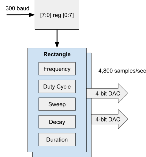
ChipTune Operation
The audio portion of the project consists of two rectangular pulse generators. Each module is controlled by four 8-bit registers. Configurable parameters are the frequency, duty cycle, sweep, decay, and note duration.
![[Operation]](https://github.com/WallieEverest/tt03/tree/main/image//tt03_chiptune.svg)
The frequency range of the project is limited by the legacy scanchain, but mid-range frequencies are acceptable. Additional triangle and noise modules will be added in future work when more bandwidth is available.
Design For Test Considerations
An isolated instance of scanchain version 2 has been tested on an FPGA platform with good results. A shift rate of 3.7 MHz permits communication with the computer at 115,200 baud. Longer scan chains do not affect throughput until multiplexer delays become dominant. For an FPGA, 75% of the timing delays are attributed to routing resources.
![[Test Configuration]](https://github.com/WallieEverest/tt03/tree/main/image/tt03_test.svg)
Output of the sub-project is always available at both the parallel output port and the serial data. A 'Mode' signal driven by the DTS line controls whether the project's input is derived from the parallel input port or serial data.
Summary
The next shuttle for TinyTapeout is planning a multiplexer for selecting between the 250 projects. This will alleviate latency in the present design. The revised scanchain offered here is an alternative for other group projects. The scanchain topology still holds merit in many applications, especially for the application of a computer-based logic analyzer via a USB COM port.
How to test
The ChipTune project can be interfaced to a computer COM port at 300 baud.
The project's scanchain is updated at 9600 Hz such that a 4800 Hz UART clock is available at io_in[4].
The system clock on io_in[0] may also be 4800 Hz.
An external bit clock must be provided on io_in[5] with a rising edge in the center of the bit period.
This clock may be sourced from the bit-aligned reference clock on io_out[5].
Serial data is received on io_in[7].
Serial data is decoded by the device as an address when io_in[6] = 0, and as data when io_in[6] = 1.
A 4-bit DAC output is available on io_out[4:0].
The mode pin, io_in[3] must stay high for this version of the design.
External hardware
Computer COM port
IO
| # | Input | Output |
|---|---|---|
| 0 | io_in[0] (CLOCK) | io_out[0] (DAC_0) |
| 1 | io_in[1] (IN_1) | io_out[1] (DAC_1) |
| 2 | io_in[2] (IN_2) | io_out[2] (DAC_2) |
| 3 | io_in[3] (MODE) | io_out[3] (DAC_3) |
| 4 | io_in[4] (BAUD_CLK) | io_out[4] (DAC_4) |
| 5 | io_in[5] (TCK) | io_out[5] (REF_CLK) |
| 6 | io_in[6] (TMS) | io_out[6] (RTCK) |
| 7 | io_in[7] (TDI) | io_out[7] (TDO) |