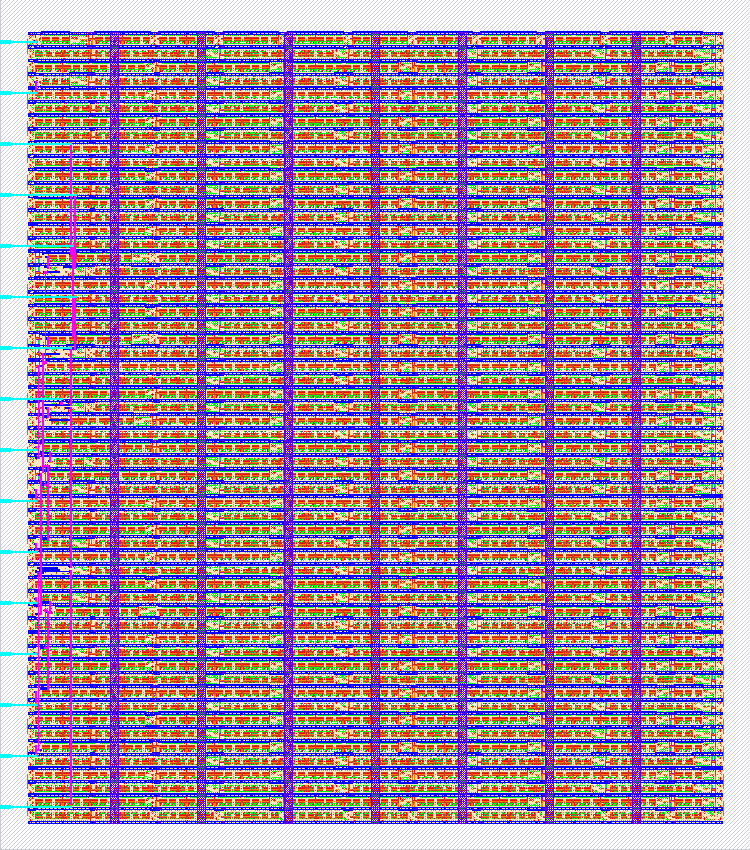
108 Logic-2G97-2G98
108 : Logic-2G97-2G98

- Author: Sirawit Lappisatepun
- Description: Replication of TI's Little Logic 1G97 and 1G98 configurable logic gates.
- GitHub repository
- Open in 3D viewer
- Clock: 0 Hz
How it works
This design replicates the circuit inside a TI configurable logic gates 74xx1G97 (and by including an inverted output, it will work as a 74xx1G98 as well). Since there are still I/O pins left, I included two of these configurables, and also one 74xx1G79 D Flip-Flop (again, an inverted output means this will also work as a 74xx1G80).
How to test
You could refer to TI's 1G79/1G80/1G97/1G98 datasheet to test the device according to the pinout listed below.
IO
| # | Input | Output |
|---|---|---|
| 0 | dff_clock | dff_out |
| 1 | dff_data | dff_out_bar |
| 2 | gate1_in0 | gate1_out |
| 3 | gate1_in1 | gate1_out_bar |
| 4 | gate1_in2 | gate2_out |
| 5 | gate2_in0 | gate2_out_bar |
| 6 | gate2_in1 | |
| 7 | gate2_in2 |