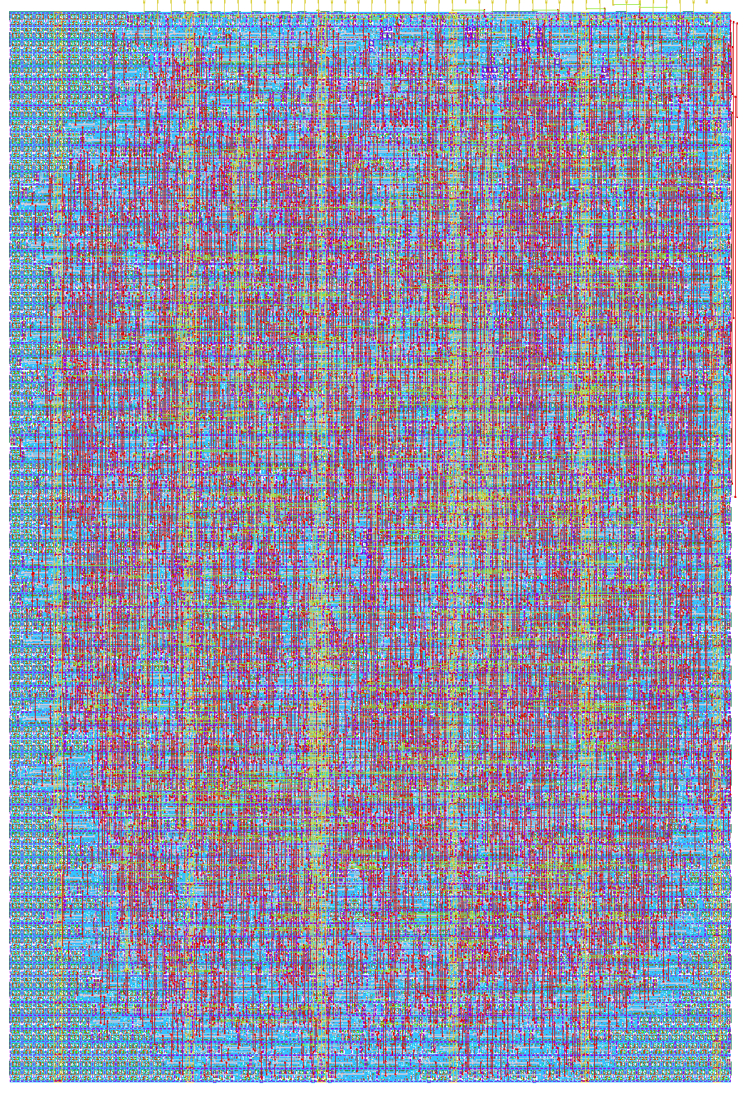
33 ROTFPGA v2b
33 : ROTFPGA v2b

- Author: htfab
- Description: A reconfigurable logic circuit made of identical rotatable tiles
- GitHub repository
- Open in 3D viewer
- Clock: 10000000 Hz
How it works
This design is a minor modification of ROTFPGA v2a, intended as a "control group" for testing latches on IHP. If ROTFPGA v2b works but v2a doesn't, it indicates an issue with latches. Otherwise it might be a problem with the design itself.
Most of the documentation carries over from ROTFPGA v2a and is not repeated here. The differences are:
- Latches are simulated using flip-flops
- Some inputs are combined to make room for two extra inputs
Simulation of latches
Latches are replaced with flip-flops that operate on the "latch clock" whereas original flip-flops are modified to act on the "flop-flop clock".
In practice the "latch clock" and the "flip-flop clock" are gated versions of clk,
enabled by in_l_gate and in_ff_gate respectively.
Input reshuffling
To add in_l_gate and in_ff_gate to the inputs, the number of existing inputs had to be
reduced. Since in_cfg is typically only used when in_se is high and in_lbc is
typically only used when in_se is low, they were combined into in_cfg_lbc.
How to test
The changes above were incorporated into the test suite. Every clock tick in the original test was replaced by 50 "latch clocks" followed by a single "latch and flip-flop clock" and then by 50 more "latch clocks".
External hardware
None
IO
| # | Input | Output | Bidirectional |
|---|---|---|---|
| 0 | tile(0,0) left in | tile(7,0) right out | _scan enable_ input |
| 1 | tile(0,1) left in | tile(7,1) right out | _scan chain_ input |
| 2 | tile(0,2) left in | tile(7,2) right out | _configuration_ / _loop breaker class_ input bit 0 |
| 3 | tile(0,3) left in | tile(7,3) right out | _configuration_ / _loop breaker class_ input bit 1 |
| 4 | tile(0,4) left in | tile(7,4) right out | _loop breaker enable_ input |
| 5 | tile(0,5) left in | tile(7,5) right out | clock gating for flip-flops |
| 6 | tile(0,6) left in | tile(7,6) right out | clock gating for simulated latches |
| 7 | tile(0,7) left in | tile(7,7) right out | _scan chain_ output |