169 Stack Calculator
169 : Stack Calculator
- Author: David Siaw
- Description: A stack based 4-bit calculator featuring a 4-bit wide 8 entry deep stack and 64 bits of random access memory.
- GitHub repository
- Open in 3D viewer
- Clock: 1000 Hz
How it works
The stack calculator is a 4-bit calculator. It is meant to be used in a larger circuit that will handle timing and memory. It is not a processor since it does not contain a program counter or attempt to access memory on its own. Rather, it accepts inputs in particular sequences and gives outputs depending on the instructions provided.
The stack calculator consists of a 4-bit wide stack that is 8 entries deep. The thing that makes it a stack calculator is the fact that all operations are performed against this stack. The user will provide opcodes at every upwards tick of the clock cycle to instruct the machine on what to do next.
The stack calculator can also save 16 4-bit values using the SAVE and LOAD
operations.
All opcodes are 4 bits long. Some opcodes accept one additional input that define the operation. Ops take at least 2 cycles to complete and at most 5 cycles.
Opcodes and operands are always 4-bits wide and are applied to the 4 input pins (pins 2-5) and need to be applied before the clock ticks up. In some cases they need to be held for more than one cycle for them to apply.
All input must be provided in a particular order. Below is a timing diagram that shows how to apply opcodes to the processor
Timing diagram

CLK   ___     ___     ___     ___     ___     ___
   __/   \___/   \___/   \___/   \___/   \___/   \___
     |       |       |       |       |       |
     |       |       |       |       |       |
1.   ___________     ________________________________
   _/  OP CODE  \___/ next operation ...

2.   _____________  _____________    ________________
   _/   OP CODE   \/   OPERAND   \__/ next op...

3.   _____________  _____________            ________
   _/   OP CODE   \/   OPERAND   \__________/ ...
                                 wait 1 cycle

LEGEND
1. 2-cycle opcode, no operands
2. 4-cycle opcode, 1 operand
3. 5-cycle opcode, 1 operand (PUSH)
The stack machine also features an output register that can be written to using the
OUTL and OUTH operations.
RESET PIN - Please hold the reset pin high and tick the clock at least 4 cycles to reset the machine.
MODE PINS - The input pins 6 and 7 are the mode pin. They can be used to set the output pins to output specific things depending on their value:
- 00 - show contents of the output register
- 01 - show 7-segment display of the top of the stack
- 10 - show 7-segment display of the value just beneath the top of the stack
- 11 - show the top 2 values on the stack on the low and high nibbles respectively.
The list opcodes are as follows:
- 0x1 PUSH
- Pushes a value to the stack. The value must be provided in the following cycle.
- 5 cycles - push, push, value, value, wait
- 0x2 POP
- Pops a value from the stack. The value must be provided in the following cycle.
- 3 cycles - pop, pop, wait
- 0x3 OUTL
- Copies the value on the top of the stack to the lower 4 bits of the output register.
- 2 cycles - outl, outl
- 0x4 OUTH
- Copies the value on the top of the stack to the high 4 bits of the output register.
- 2 cycles - outh, outh
- 0x5 SWAP
- Swaps the top two values on the stack.
- 3 cycles - swap, swap, wait
- 0x6 PUSF
- Push a value on the stack depending on the operand. The operand determines the values pushed on the stack.
- 4 cycles - peek/dupl/flag, =, wait
- 0x0 DUPL - pushes a copy of the value on the top of the stack to the top of the stack
- 0x1 PEEK - pushes a copy of the value below the top of the stack to the top of the stack
- 0x2 FLAG - pushes the contents of the status register
- 0x7 REPL
- Removes the value at the top of the stack and pushes the value modified by an unary operation
- 4 cycles - not/neg/incr/decr/shr1/shr2/ror1/rol1, =, wait
- 0x0 NOT - bitwise NOT
- 0x1 NEG - negative, or 2's complement
- 0x2 INCR - increment
- 0x3 DECR - decrement
- 0x4 SHR1 - shift right by 1
- 0x5 SHL1 - shift left by 1
- 0x6 ROR1 - rotate right by 1
- 0x7 ROL1 - rotate left by 1
- 0x8 BINA
- Binary operation - removes the top two values of the stack and pushes the result of a binary operation
- 4 cycles - add/and/not/xor/addc/mull/mulh, wait, wait
- 0x0 ADD - add (will set the status register carry flag if result > 15)
- 0x1 AND - bitwise AND
- 0x2 OR - bitwise OR
- 0x3 XOR - bitwise XOR
- 0x4 ADDC - add with carry. same as add but +1 if carry flag is set
- 0x5 MULL - low nibble from result of multiplication
- 0x6 MULH - high nibble from result of multiplication
- 0x9 MULT
- Full multiply of the top two nibbles on the stack. Pushes the high nibble and then the low nibble to the stack in that order.
- 4 cycles - mult, mult, wait, wait
- 0xA IDIV
- Divide the value below the top of the stack by the value on the top of the stack. Pushes the remainder and the integer division result in order.
- 4 cycles - idiv, idiv, wait, wait
- 0xB CLFL
- Unset all flags in flag register
- 4 cycles - clfl, clfl
- 0xC SAVE
- Writes the value below the top of the stack to the address provided at the top of the stack.
- 4 cycles - save, save, wait, wait
- 0xD LOAD
- Loads the value at the address provided at the top of the stack.
- 4 cycles - load, load, wait, wait
How to test
The following diagram shows a simple test setup that can be used to test the stack calculator
  VCC
  |    __|__ pushbutton
  +----.   .-------------+
  |                     _|_
  |          schmitt    \ /
  |          trigger     O
  |          inverter    |
  |  __|__               +--> CLK  OUT0 -----+
  +--.   .------------------> RST  OUT1 -.   |
    button     +--------+---> IN0    .      _|_
               +        +---> IN1    .      \ / buffer
               +        +---> IN2    .       |
               +  DIP   +---> IN3            |
               + switch +---> MODE0          +--> 7 segment
               +        +---> MODE1          |
               +        +--                  +--> LED bar array
               +--------+--
                                              .
                                              .
                                              .
By using a schmitt trigger for debounce and an inverter, it is possible to perform a tick up with a specific DIP switch setting, allowing us to experiment with different kinds of inputs in sequence.
Using the DIP switch you can also change the MODE pins to debug your stack or display the output register contents.
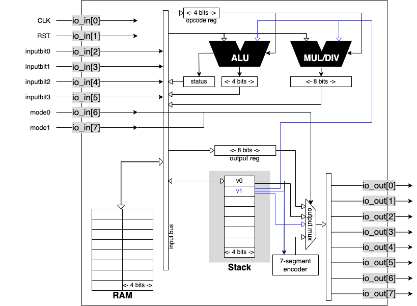
IO
| # | Input | Output |
|---|---|---|
| 0 | clk | output0 |
| 1 | rst | output1 |
| 2 | input0 | output2 |
| 3 | input1 | output3 |
| 4 | input2 | output4 |
| 5 | input3 | output5 |
| 6 | mode0 | output6 |
| 7 | mode1 | output7 |