FAQ
Support
I’m stuck, how can I get support?
Join the discord community with this link.
Chip Specs for TT04 to TT10
What is the top clock speed?
At least 50MHz. We have received silicon for our test run and are in the process of measuring it.
How many ins and outs do I get?
- clock and nreset (low to reset)
- 8 ins
- 8 outs
- 8 bidirectional IOs
What PDK is used for the manufacture?
We are using the open source Skywater 130nm PDK
How big can my design be?
For TT04 to TT10, the standard tile size is about 160x100 um. This is enough for about 1000 digital logic gates, depending on their size. You can also buy extra tiles if you need more room.
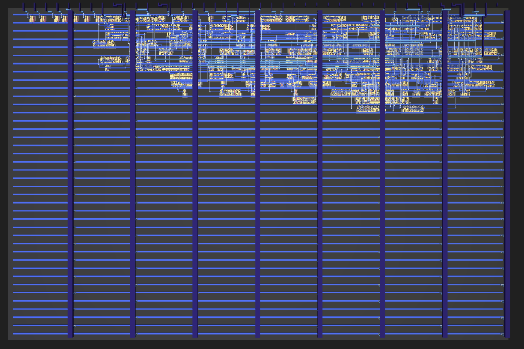
Here’s a 3D view of the GDS of my 7 segment seconds counter, a small design that increments a counter every second and shows the result on the 7 segment display.
Click the picture to open an interactive viewer.
When will the chips get manufactured?
The chips are taking between 6 and 9 months to manufacture. Then we need to do PCBA, test and order fulfillment. So expect up to 1 year’s wait time!
You can find an up to date estimate for each shuttle in the chips page.
Purchasing / Product FAQs
What is the price?
You can use our handy calculator to check pricing.
How many chips will I receive? Can I order more?
You only get 1 chip. If you want more chips you have to order more of the devkit PCBs - the early bird price is only available once per person.
What is a ‘devkit’?
A devkit (short for development kit) (also stylised as DevKit or dev-kit) is a set of components that provide an interface to the shuttle’s ASIC. The devkit consists of two PCBs (printed circuit boards) - a ‘demo board’ and a ‘breakout board’.
The breakout board contains the shuttle’s ASIC, and connects to the demo board via a set of pins. The demo board contains a microcontroller and relevant firmware for you to interface with it via the Tiny Tapeout Commander. The demo board also contains additional connectors and components (LEDs, 7 segment display, DIP switches) for you to interact with.
The devkit we provide is a pre-assembled board, so it is ready for you to use as soon as you receive it. There are no plans to provide a DIY devkit, however the files are available on GitHub (github.com/TinyTapeout/tt-demo-pcb).
When you purchase 1 devkit, you will receive 1 demo board and 1 breakout board.
What is an ‘analog slot’?
An analog slot is 1x2 tiles large, and there are a limited number of available slots per shuttle. Availability of analog slots can be seen via the shuttle status page.
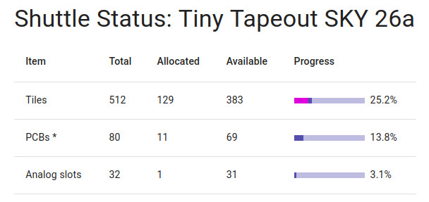
Availability of analog slots on TTSky26a
An analog project can take up a maximum of two analog slots - therefore valid sizes for analog projects are either 1x2 or 2x2. Tiles may be slightly smaller if using the 3V3 power gate.
If you require a larger size, you will be charged as if you had submitted multiple 1x2/2x2 projects separately. For example, if you wanted 3x2 tiles and 4 pins for a single project, you’ll be charged for 2x2 tiles + 4 pins, then 1x2 tiles + 4 pins - even if you are only using 4 pins for your project.
Can I buy older chips?
Leftover chips and PCBs get put into our shop. We only sell spares, so there is no guarantee there will be any.
Can I get the chip by itself?
Unfortunately no. We don’t ship bare dies either. The best way to get access to a chip is to pre-order a devkit and desolder the chip from the breakout board, or to wait for an ASIC kit (see our TT07 one as an example) to appear in the shop. ASIC kits aren’t guaranteed for every shuttle.
Some shuttles (such as our GF180-based ones) don’t come with a traditionally packaged chip - they instead have the die bonded to a PCB directly (called chip-on-board, or COB) and therefore cannot be removed.
If you are designing a PCB and wish to use a Tiny Tapeout chip, then we recommend that you design your PCB to interface with our breakout board - it will provide you with 2 connectors where you get all of the signals of the chip. See our breakout board schematics on GitHub.
If your goal was to save money by ordering the chip by itself, then you would be saving very little - a significant portion of the costs stem from the chip itself, along with all the logistics and handling related to it. The cost of the PCB components is minimal compared to the ASIC itself.
Wokwi FAQs
How do I do x, y, z with Wokwi?
Wokwi’s documentation is here. We don’t have much documentation yet for the ASIC version of Wokwi.
Shortcut keys
- select a component and press delete to remove it
- select a component (or shift select to add more components), then d to duplicate it.
- shift and drag to drag a box around multiple components
-
- and - to zoom in and out
- More here.
Can I copy and paste from one Wokwi design to another?
- Select all the parts you want to copy (using shift and click the parts or shift and drag a box)
- Copy them to clipboard (Ctrl+C or Cmd+C)
- Go to the target project, click on the diagram editor, and paste (Ctrl+V or Cmd+V)
How can I undo / redo?
- Ctrl+Z & Ctrl+Y or ⌘Z / ⌘Y on a Mac.
How do I find out the wiring of the 7 segment display?
Clicking on a component will bring up a ? in a circle. Click on the ? to get the help.
Do I have to use the 7 segment?
No, you can delete it and put whatever you want there. There’s lots of other components you can choose from the + menu. But if you get a PCB, it will only have the 7 segment on it. You’d need to plug the board into a breadboard and add your extra components after.
How do I add new gates?
Either duplicate an existing one (select it and press d), or:
- press the + button menu at the top of the page,
- in the filter box, type ’logic’ to filter only the logic gates.
How do I move a set of gates?
Select all the ones you want to move (using shift and click the parts or shift and drag a box). Then drag the selection.
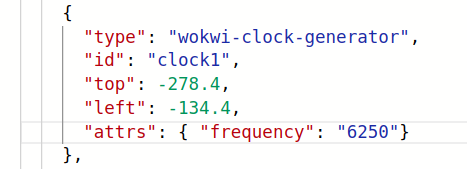
How do I use the clock block?
You can use the first input as the clock. If you need to change the clock frequency you have to do it by editing the json diagram file. Set the “frequency” attribute to the frequency you want in Hz (e.g. “10000” or “10k” for 10 KHz).
Tiny Tapeout will support a wide range of clock frequencies (we anticipate up to 50 MHz). However, to make sure Wokwi simulates your design fast enough, you should not use a clock frequency higher than 100 KHz while simulating your design.
Are there some examples of projects people have made?
Check the chips page.
Do I need to delete unused digital gates?
No, unused gates will be optimised out by the ASIC tools.
I found and fixed a problem in my design - do I need to resubmit?
Yes, you need to
- re-run the github action.
- Tell us to use your latest version using the Tiny Tapeout application.
Do I need to use Wokwi, or could I use an HDL?
If you’re an advanced user, you can use the HDL of your choice. See the HDL page for more information.
My Wokwi design fails with an “unmapped dff cell” error - what do I do?
You may be using an unsupported flip flop configuration in a project which is targeting the IHP PDK. Depending on your
circuit, the quickest fix may be to replace all instances of wokwi-flip-flop-dsr with wokwi-flip-flop-dr within the
diagram.json file. This does mean that you lose the set functionality of the flip-flop, so it may not always be suitable.
Tiny Tapeout FAQs
Where can I find the the template to get started?
You can access it on the Getting Started Page.
Which of my builds will be submitted for fabrication?
If you update your project and want us to use your latest version, you have to go to your submission and create a new submission.
You can keep updating your design up to the tapeout deadline.
Submission fails asking to reharden the project for the correct PDK - how do I do this?
Example error message:
This project was hardened for sky130A, but you are trying to submit it to a shuttle using ihp-sg13g2. Please reharden the project for the correct PDK and try again.
This error message appears when you have hardened your design for one process, but are attempting to submit onto a shuttle which uses a different process. In the example above, the project was hardened with the SkyWater PDK, but is being submitted on an IHP shuttle - the manufacturing process is different and therefore the submission fails.
To fix this you can either:
- Migrate your source files onto the correct project template
- Copy all the files from the correct template into your existing repo
- These should replace anything in
.github/workflows,.devcontainerandtest/Makefile
- These should replace anything in
Is it TinyTapeout or Tiny Tapeout?
It’s Tiny Tapeout. See the Branding page for more information.
Github FAQs
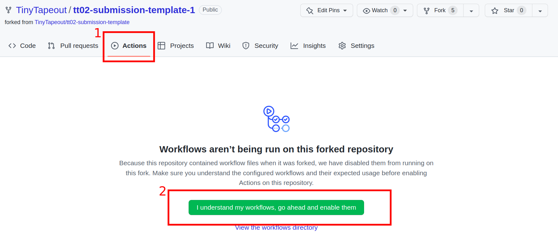
When I commit my change, the GDS action isn’t running
You need to enable the actions.
- Go to the Actions tab,
- Click the enable actions button.
Also see the next FAQ on the GDS action failing on ‘pages’.
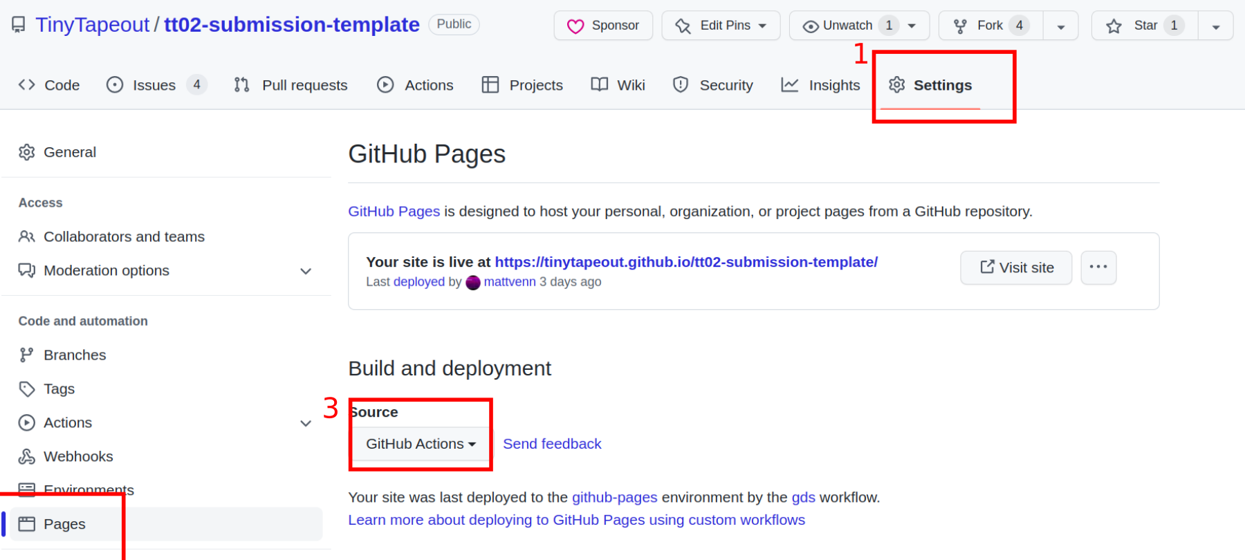
My GitHub action is failing on the ‘pages’ part.
Due to Github limitations, you need to do make a change to the settings of your repository to get everything to work.
- Go to Settings tab,
- Select Pages,
- Change Source from Deploy from a branch to GitHub Actions.
I got an error on my GitHub GDS action.
The best way to let me know is to ask a question in our community discord chat, in the #questions channel. Include a link to your repository and the error message.
I got an error on my GitHub Documentation action.
You might not have filled in enough fields, we require the following fields to be filled:
author
title
description
how_it_works
how_to_test
language
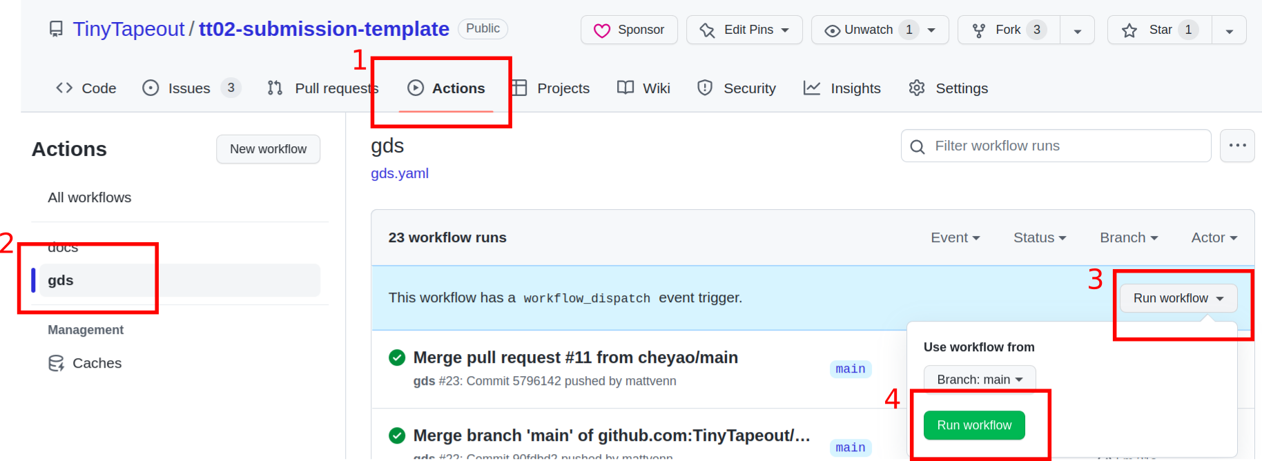
I updated and saved my Wokwi design, how do I re-run the Github action to update the GDS files?
- Go to your repository, click the actions tab
- Then click the ‘gds’ workflow
- Then click the ‘Run workflow’ button
- Then click the ‘Run workflow’ button
What are all the files in the artifact?
There are lots!
- src - the source files for your chip:
- user_module_xxxxx.v the Verilog file that represents your Wokwi design.
- config.tcl - config file for the OpenLane ASIC tool flow that turns the Verilog into GDS.
- cells.v translates the modules into the standard cells available for the Skywater 130nm process.
- runs/wokwi/reports/metrics.csv - a detailed summary report of the tool flow. It’s beyond the scope of this doc for now to explain it all.
- runs/wokwi/reports/synthesis/1-synthesis.stat.rpt.strategy4 report of the standard cells used for your design.
- runs/wokwi/results/final/ (just the most important described here)
- gds - the final GDS file that will be added to the Tiny Tapeout submission.
- lef - an abstract version of the GDS with less information, used for routing.
- verilog - the gate level verilog of your design.
ASIC FAQs
What do all these acronyms you keep using mean?
Sorry! We are trying to keep it accessible but we’ll inevitably use some ASIC terminology at some point! See the terminology guide here.
Why do I have fewer / more standard cells than I expected?
Logic synthesis has to convert Verilog to a data structure which has specific properties so that a technology library (like Sky130) can be mapped to it, so that it can actually be fabricated.
If you have 2 inverters in series, Yosys (the synthesis tool) may well optimise them both out, so you end up with less cells than expected.
However, if you have only 8 cells, your design is probably completely optimised out. Maybe you didn’t connect the inputs or outputs?
Why is target density set to 60%? Should I change it to 100% or should I add another tile?
Routing tends to take up more space than the logic. Also, there needs to be space for OpenLane to add extra cells:
- tap cells - make sure the substrate is correctly biased for the transistors.
- antenna diodes - protect transitor gates during manufacture.
Some people have successfully increased the target density to around 62%. Alternatively you can buy an additional tile.
How can I learn more about ASICs and how to design them?
Check out Matt’s Zero to ASIC course!
How can I map an additional external clock to one of the GPIOs?
Tiny Tapeout provides a set of 24 general-purpose I/O pins: 8 are input-only (ui_in), 8 are output-only (uo_out) and 8 are tri-state bi-directional (uio_*).
By default, the clk input port is used as the main clock, generated by the on-board RP2040 chip. However, it is possible to use one of the inputs ui_in as auxiliary clock. In this
case, special care must be taken when running the flow.
As an example, let’s assume two clocks are needed: the one generated by the RP2040 device, we name it rp2040_clk, and an auxiliary one generated by an off-board FPGA, we name it fpga_clk.
Both clocks have the same frequency, but clearly unknown phase (i.e., they are mesochronous). Also, let’s assume these clocks do never interact each other (i.e., no CDC). We also map
the fpga_clk to pin ui_in[0].
To be able to run this scenario we need to tweak the configuration file config.tcl that will be used by the Tiny Tapeout workflow, so that:
- We instruct OpenLane to generate two clock trees, and not just the one related to the
clkport; - We tell OpenLane the two clocks are physically separated.
The following lines are required in the config.tcl file:
1 set ::env(CLOCK_PORT) "ui_in\\\[0\\\]"
2 set ::env(BASE_SDC_FILE) "$::env(DESIGN_DIR)/project.sdc"
Line 1 sets the CLOCK_PORT name, from the (default) clk to our ui_in[0]. Please notice the backslash pattern here! There is no need to set the CLOCK_NET variable to a list of clocks,
since we are using a custom constraint file, namely project.sdc.
Then, the contents of project.sdc are:
 1 # Shared constants, copied from  base.sdc
 2 set input_delay_value [ expr $::env(CLOCK_PERIOD) * $::env(IO_PCT) ]
 3 set output_delay_value [ expr $::env(CLOCK_PERIOD) * $::env(IO_PCT) ]
 4 set_max_fanout $::env(MAX_FANOUT_CONSTRAINT) [ current_design ]
 5 set cap_load [ expr $::env(OUTPUT_CAP_LOAD) / 1000.0 ] ;# fF -> pF
 6
 7 # Remove clock net from inputs
 8 set idx [ lsearch [ all_inputs ] "clk" ]
 9 set all_inputs_wo_clk [ lreplace [ all_inputs ] $idx $idx ]
10 set idx [ lsearch $all_inputs_wo_clk "ui_in\[0\]" ]
11 set all_inputs_wo_clk [ lreplace $all_inputs_wo_clk $idx $idx ]
12
13 #  clk   clock is generated by the RP2040 chip
14 create_clock [ get_ports "clk" ]  -name rp2040_clk -period $::env(CLOCK_PERIOD)
15 set_input_delay $input_delay_value -clock [ get_clocks rp2040_clk ] $all_inputs_wo_clk
16 set_output_delay $output_delay_value -clock [ get_clocks rp2040_clk ] [ all_outputs ]
17 set_clock_uncertainty $::env(SYNTH_CLOCK_UNCERTAINTY) [ get_clocks rp2040_clk ]
18 set_clock_transition $::env(SYNTH_CLOCK_TRANSITION) [ get_clocks rp2040_clk ]
19
20 #  ui_in[0]   clock is generated by the FPGA
21 create_clock [ get_ports "ui_in\[0\]" ]  -name fpga_clk -period $::env(CLOCK_PERIOD)
22 set_input_delay $input_delay_value -clock [ get_clocks fpga_clk ] $all_inputs_wo_clk
23 set_output_delay $output_delay_value -clock [ get_clocks fpga_clk ] [ all_outputs ]
24 set_clock_uncertainty $::env(SYNTH_CLOCK_UNCERTAINTY) [ get_clocks fpga_clk ]
25 set_clock_transition $::env(SYNTH_CLOCK_TRANSITION) [ get_clocks fpga_clk ]
26
27 # rp2040_clk  and  fpga_clk  are mesochronous, and they never interact
28 set_clock_groups -asynchronous -group { rp2040_clk } -group { fpga_clk }
29
30 # Miscellanea
31 set_driving_cell -lib_cell $::env(SYNTH_DRIVING_CELL) -pin $::env(SYNTH_DRIVING_CELL_PIN) $all_inputs_wo_clk
32 set_load  $cap_load [ all_outputs ]
33 set_timing_derate -early [ expr {1-$::env(SYNTH_TIMING_DERATE)} ]
34 set_timing_derate -late [ expr {1+$::env(SYNTH_TIMING_DERATE)} ]
Please be careful of the backslash pattern here! It is different than the config.tcl case! If you run into the following error:
[ERROR]: The specified clock port 'ui_in[0]' does not exist in the top-level module.
chances are the backslashes are wrong!
The above SDC is pretty much derived from the default base.sdc constraint file. Please remember once again that the two clocks have same frequency! The file has been organized, though:
- Clock-unrelated values are computed first. This works if and only if the two clocks have the same frequency!
- The
rp2040_clkis generated first, with its own I/O delay and uncertainty; - The
fpga_clkis generated next; - The two clocks are said to be independent;
- Miscellanea settings (e.g., timing derate) follow.
With the above two clock trees are generated, STA analysis will be run on both clock trees and no CDC shall be found.
Please note that the above works for OpenLane tag 2023.11.23. More recent versions that include the check_clock_ports.py script will not work. This is due to the way the
check_clock_ports.py works: it is not able to detect sliced ports (as in ui_in[0]).
Can I use a different HDL instead of Verilog?
There is some support for VHDL, but the open-source tools are mainly geared towards Verilog so some features may not
work as expected. You can get started with VHDL via our Verilog template and simply specify your VHDL source files in
info.yaml. The build action will convert your VHDL source files into Verilog individually via GHDL. This comes with
downsides however - you won’t be able to use any custom types or records, and you will have to treat each module
instanciation as a black box.
There is a Chisel template available (thanks to Martin Schoeberl!): github.com/TinyTapeout/ttihp-chisel-template