130 Antonalog analog VGA
130 : Antonalog analog VGA
- Author: algofoogle (Anton Maurovic)
- Description: Rough 24-bit VGA DAC tests with digital control block
- GitHub repository
- Open in 3D viewer
- Open in VGA Playground
- Clock: 25000000 Hz
- Feedback: 🟡 1
Overview
For a quick-start guide on simply testing the RDAC performance in this design using an oscilloscope, just see the heading "1. Measure analog outputs on an oscilloscope". I intend to have results collected in the TTIHP0p3-Antonalog sheet of my "Anton's Tiny Tapeout silicon testing" Google Sheet.
This mixed-signal design uses 3 instances of an 8-bit RDAC to produce analog voltage outputs for each of the red, green, and blue channels of a video display. It was submitted to TTIHP0p3, and the specific commit workflow was: https://github.com/algofoogle/ttihp0p3-antonalog/actions/runs/15096423059
The output range of the DACs is 0-1.2V (or whatever core voltage you provide to the chip).
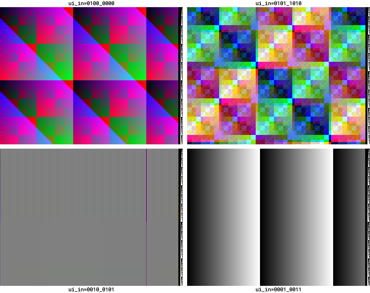
This design provides simple ways to just test the performance/linearity/slew of the DACs, but also includes a digital control block that generates various VGA display test patterns, some of which are demonstrated above. Besides the analog outputs, the uo_out port is also compatible with the Tiny VGA PMOD (providing just RGB222 instead of the design's full RGB888 capability).
NOTE: The output impedance of the DACs is about 8660Ω (i.e. internally, the RDACs use R ≈ 8660Ω).
Quick start
Take your pick from the options below:
- Use an oscilloscope, with the design's modes for measuring linearity or slew rate for any/all of the analog RGB outputs.
- Plug in a Tiny VGA PMOD and just see the VGA pattern generator doing something.
- Generate full RGB888 images on a VGA display by buffering/shifting the analog outputs with op-amps.
1. Measure analog outputs on an oscilloscope
Basic setup common to all measurements done with a scope:
- To sync to the start of each frame, set your scope to trigger on the rising edge of
vblank_out(uio_out[0]). - Probe any (or all) of the analog outputs:
r(red, onua[0]),g(green, onua[1]), orb(blue, onua[2]). - Supply a 25MHz clock; this will conveniently make each DAC output sample 40ns in duration.
- Set
ui_into one of the test modes as described below (00010011, i.e. 0x13, is good to start with). - Assert reset.
During reset, the design will latch the test mode specified by ui_in. Some of these modes include:
-
00010011(0x13): All 3 analog output channels ramp up together at a rate of 40ns per level, i.e. they all start at 0 (0V), increment per-pixel to eventually reach 255 (~1.2V), then after 256 clocks (10.24µs) will start again from 0. This allows simple measurement of:- The slew rate from one level to the next
- The full-swing rate back down to 0
- Any non-linearity or discontinuities in the ramp
-
00010000(0x10): Red ramps at the full per-pixel rate, Green ramps per-line, and Blue ramps per-frame. In this mode, cross-talk between channels might become evident. -
00100000(0x20): "Bars" mode: Same as above (0x10) but the output is inverted on every odd pixel. This allows measurement of big swings both up and down.
NOTE: All modes output the line number, as a binary pattern (black and white pixels), in the last 16 pixels of each line.
2. Tiny VGA PMOD output
- Attach a Tiny VGA PMOD to the
uo_outport, and plug in a VGA monitor. - Supply a 25MHz clock.
- Set
ui_into (say)01010000(0x50). - Assert reset.
- Expect to see a pattern like the one shown in the top-right screenshot above, though with much-reduced bit depth (per the limited RGB222 output of the Tiny VGA PMOD).
3. Full analog VGA display
- Use 3 op-amps on the analog outputs to both buffer them (matching 75Ω termination of the VGA monitor's colour channels) and level-shift them to 0-0.7V (instead of 0-1.2V). The OPA3355 is a good choice: it comprises 3 op-amps that are fast enough for VGA, and are (moderately) rail-to-rail to use with (say) a single 3.3V supply.
- Optionally buffer the
hsyncandvsyncoutputs and use (say) 50Ω in series with the respective VGA monitor inputs. - Per "2. Tiny VGA PMOD output" above, set up the design and select a
ui_inmode.
Test modes on ui_in
There are lots of different options for the ui_in test modes, including some which are intentionally sensitive to a change in ui_in value after initial latching at reset. For details, see my explanation of the digital control block's inputs, but here's a quick version of the more-useful modes:
00010000: Red channel ramps per pixel, Green channel ramps per line, Blue channel ramps per frame.00010011: All 3 channels ramp per pixel (i.e. grey ramps). See bottom-right screenshot above.00100000: "Bars" mode: Same as00010000except that every odd-numbered pixel gives an inverted output. Note that the 4 LSBs set different options (as they do for the above 2 modes); see bottom-left screenshot above.01000000: "Classic" XOR mode, seen in the top-left screenshot.01010000: "New" XOR mode, seen in the top-right screenshot.01100000: A static (non-animated) version of the "New" XOR mode.00000000: Pass-through mode: In this mode, after reset any value presented onui_inwill be passed directly through to all 3 DACs. NOTE: Ifui_in[1]is 0, then the output is ungated, otherwise if 1 the output is gated to only be passed through during the visible portion of each frame.
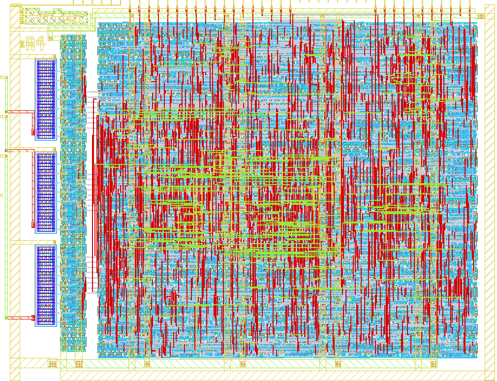
Design
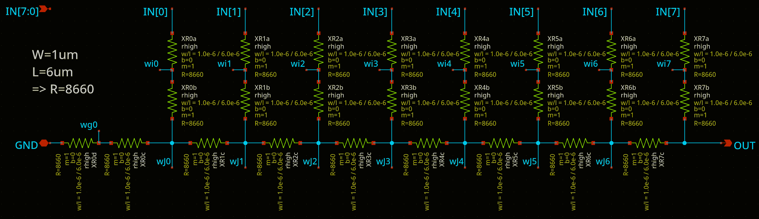
Each of the 3 DAC instances uses a typical R2R DAC, where R ≈ 8660Ω.
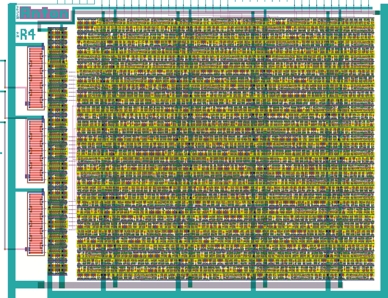
In the layout above:
- There is the main digital control block occupying most of the area (i.e. on the right).
- To the left of that is a thin column of digital layout which just implements uniform drivers for the RGB888 signals into the DACs using
sg13g2_buf_8cells. - To the left of that are the 3 instances of the RDAC layout. It uses resistors of matched sizes, i.e. where "2R" is required, there is a pair of "R"-sized resistors in series.
Background
This was my first attempt at a custom layout and mixed-signal design on IHP SG13G2.
I leaned heavily on https://github.com/htfab/ttihp0p3-r2r-dac for the analog layout parts of this, and the digital control block is from my earlier tt08-vga-fun project. For my related VGA DAC projects, see:
- Write-up on my original TT06 analog VGA driver.
- TT08 VGA FUN! -- An alternative design trying out current-steering and current-switching DAC designs.
- TTSKY25a Analog VGA CSDAC experiments -- A current-switching DAC matrix, first attempt.
- TTSKY25b Analog VGA CSDAC experiments -- 2nd attempt at the DAC matrix, fixing some performance issues with the TTSKY25a version. In particular, this version has better parasitics and a 'registered' mode.
IO
| # | Input | Output | Bidirectional |
|---|---|---|---|
| 0 | mode[0] / dac_in[0] | r7 | vblank_out |
| 1 | mode[1] / dac_in[1] | g7 | hblank_out |
| 2 | mode[2] / dac_in[2] | b7 | |
| 3 | mode[3] / dac_in[3] | vsync | |
| 4 | mode[4] / dac_in[4] | r6 | |
| 5 | mode[5] / dac_in[5] | g6 | |
| 6 | mode[6] / dac_in[6] | b6 | |
| 7 | mode[7] / dac_in[7] | hsync |
User feedback
- mattvenn: Some patterns show fine, some are fairly distorted, sometimes the VGA screen loses sync. analog output looks good, took a bunch of scope shots in the different test modes and shared via discord. Link for more details