257 SONOS Flash Party
257 : SONOS Flash Party
- Author: Uri Shaked, Aidan Medcalf
- Description: Experimental SONOS Flash controller for Tiny Tapeout
- GitHub repository
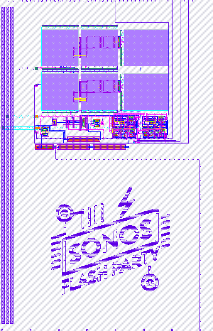
- Open in 3D viewer
- Clock: 0 Hz
How it works
An experiment in creating a functional SONOS flash storage device for Tiny Tapeout (SkyWater 130 nm process).
We generate two internal voltages using charge pumps, and use them to program and erase the flash:
vprgposis at 7.4V, generated using a two-stage charge pump from the VAPWR (3.3V supply).vprgnegis at -4.5V, generated using a two-stage charge pump from the VAPWR (3.3V supply).
The prog_en and erase_en inputs control how we apply these voltages to the SONOS flash cell:
prog_en |
erase_en |
SONOS gate | SONOS body | Description |
|---|---|---|---|---|
| 1 | 0 | 7.4V | -4.5V | Programming |
| 0 | 1 | -4.5V | 7.4V | Erase |
| 0 | 0 | 0V | 0V | Read / No operation |
| 1 | 1 | 7.4V | 7.4V | Invalid state |
In summary, we apply about 11.9V to the SONOS gate and body when programming, and -11.9V when erasing (we'll get a more accurate value once we have a post-layout simulation).
The read_en connects the source of the SONOS gate to the ground, and weakly pulls the SONOS drain to the VDPWR (1.8V supply). When the SONOS is erased, the drain is pulled towards 0V. When the SONOS is programmed, the drain is pulled towards 1.8V. We buffer the drain with an inverter to get a clean digital output, which is available on the data_out pin. The following table summarizes the behavior of the data_out pin:
| State | read_en |
Drain voltage | data_out |
|---|---|---|---|
| Erased | 1 | ~0.51V | 1 |
| Programmed | 1 | 1.8V | 0 |
| any | 0 | undefined | undefined |
Note: all of the voltages above were obtained from pre-layout simulations, and are approximate.
The charge pump voltage is divided by about 3.5 and available on the vprogmon analog output (should be around 2.11V, according to simulation).
How to test
Clock the design with a 2 MHz clock. Observe the generated voltage on the vprogmon (ua[0]) analog output. If you see about 2.11V, the charge pump is working correctly.
To program the flash (set the data to 0), pulse prog_en high for about 10 miliseconds. To erase the flash (set the data to 1), pulse erase_en high for about 15 miliseconds. In both cases, the charge pump needs to be clocked with a 2 MHz clock.
Read the flash by pulsing read_en high for about 100ns, and observe the data_out digital output. It is not required to clock the charge pump while reading the flash, but it is not harmful either.
Note: the pulse width and clock frequency above are just rough estimates. More accurate values will be determined in the future, once we get the silicon back.
External hardware
None
IO
| # | Input | Output | Bidirectional |
|---|---|---|---|
| 0 | prog_en | data_out | |
| 1 | erase_en | ||
| 2 | read_en | ||
| 3 | |||
| 4 | |||
| 5 | |||
| 6 | |||
| 7 |
Analog pins
ua | PCB Pin | Internal index | Description |
|---|---|---|---|
| 0 | B1 | 7 | vprogmon |