271 4-Bit Successive Approximation ADC
271 : 4-Bit Successive Approximation ADC
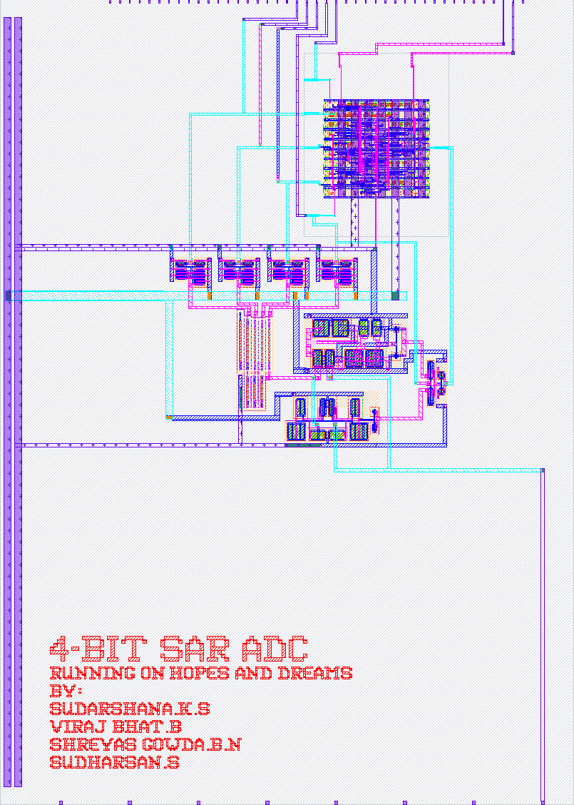
- Author: Sudarshana K S, Viraj Bhat B, Shreyas Gowda B N, Sudharsan S, Shylashree N, RV College of Engineering
- Description: This project implements a 4-Bit Successive Approximation Analog-to-Digital Converter
- GitHub repository
- Open in 3D viewer
- Clock: 5000000 Hz
Credits :
We sincerely acknowledge the Center of Excellence in Integrated Circuits and Systems(CoE-ICAS) and the Department of Electronics and Communication Engineering, RV College of Engineering, Bengaluru, for their invaluable support in providing us with their knowledge and training.
We extend our special gratitude to Dr. M Uttara Kumari (Dean of Research and Development), Dr. Ravish Aradhya H V (HoD, ECE), Dr. K S Geetha (Vice Principal), Dr. K N Subramanya (Principal) and Rashtreeya Sikshana Samithi Trust for their constant support and encouragement, which enabled us to design a tapeout for Tiny Tapout 10.
Description
The 4-Bit SAR ADC operates by efficiently converting Analog continous time data to Digital bit stream, enabling seamless interfacing between Analog and Digital systems at high speeds. Here's how it works:
-
Successive Approximation Register (SAR):
- The SAR is the core block of our ADC design, performing a binary search in each conversion cycle to accurately match the analog input
Vinto its corresponding digital level. - It performs successive approximation, adjusting the DAC output iteratively based on the bit-wise output of the comparator.
- The SAR is the core block of our ADC design, performing a binary search in each conversion cycle to accurately match the analog input
-
R-2R Ladder Digital-to-Analog Converter:
- This block converts the digital output from the SAR into its corresponding analog value, which is then fed to the comparator as a reference.
- The DAC output must be highly accurate to minimize Differential Non-Linearity (DNL) and Integral Non-Linearity (INL) errors in the ADC.
- The DAC needs to be driven by a very low resistance Driver circuit achieved by using Wide NMOS and PMOS pair at the Input of the DAC.
-
Complementary Comparator Pair:
- A generic comparator often has a limited common-mode range, making it unreliable when comparing signals outside this range.
- An NMOS differential pair comparator fails at lower voltages, while a PMOS differential pair comparator fails at higher voltages.
- To overcome this limitation, we have designed a novel comparator structure that dynamically switches between the two comparators, allowing accurate voltage comparisons across the full range at high speeds.
Overall, the 4-Bit SAR ADC offers an efficient and reliable method for data conversion even at high speeds, enabling seamless interfacing between the Analog and Digital Domain.
How to test
Analog Input (Vin):
- Connect the analog input to the
ua_0Analog pin. - The input should be held constant throughout the conversion cycle using an external sample-and-hold circuit.
Clock (clk):
- Provide a 5 MHz clock to the clk pin.
Reset (rst_n):
- The active-low reset
rst_nmust be pulsed each time theuo_0(EOC) pin goes high.
Conversion Timing:
- Each conversion takes 5 clock cycles, resulting in a conversion frequency of 1 MHz.
Digital Output:
- The ADC output is available at the pins at the End of conversion cycle:
uo_1→ D3uo_2→ D2uo_3→ D1uo_4→ D0
External hardware
We will be using a Sample and Hold circuit to Hold the Vin constant throughout the conversion cycles.
IO
| # | Input | Output | Bidirectional |
|---|---|---|---|
| 0 | EOC | ||
| 1 | D[3] | ||
| 2 | D[2] | ||
| 3 | D[1] | ||
| 4 | D[0] | ||
| 5 | |||
| 6 | |||
| 7 |
Analog pins
ua | PCB Pin | Internal index | Description |
|---|---|---|---|
| 0 | B4 | 10 | Vin |